Semiconductor device, wireless sensor, and electronic device

a wireless sensor and semiconductor technology, applied in the direction of power saving provisions, electrical analogue stores, instruments, etc., can solve the problems of increasing power consumption, reducing the performance of ad converters, and continuously consuming power while supplied with power, so as to prolong communication distance, not decrease the performance of ad converters, and the effect of new structur

Inactive Publication Date: 2016-03-31
SEMICON ENERGY LAB CO LTD
View PDF7 Cites 42 Cited by
  • Summary
  • Abstract
  • Description
  • Claims
  • Application Information

AI Technical Summary

Benefits of technology

[0024]One embodiment of the present invention can provide a novel semiconductor device, a novel electronic device, or the like.
[0025]According to one embodiment of the present invention, it is possible to provide a low-power semiconductor device or the like having a novel structure. According to one embodiment of the present invention, it is possible to provide a semiconductor device or the like having a novel structure that does not decrease the performance of an AD converter, such as the resolution and sampling rate. According to one embodiment of the present invention, it is possible to provide a semiconductor device or the like having a novel structure that does not require a dedicated high-voltage generation circuit and a dedicated peripheral circuit for holding analog data. According to one embodiment of the present invention, it is possible to provide a wireless sensor with an AD converter or the like having a novel structure that enables extension of a communication distance.

Problems solved by technology

That is, the AD converter continuously consumes power while supplied with power.
However, decreasing a drive voltage and decreasing drive frequency are directly related to the resolution and sampling rate of the AD converter, therefore, decreasing a drive voltage or drive frequency leads to reduction in the performance of the AD converter.
In addition, intermittently supplying power is available with the use of a flash memory for holding analog data, but additionally needs a dedicated high-voltage generation circuit and a dedicated peripheral circuit, which adversely leads to increase of power consumption.
In a wireless sensor or the like including an AD converter, increased power consumption of the AD converter causes a problem such as a shorter communication distance.

Method used


Image

  • Semiconductor device, wireless sensor, and electronic device
  • Semiconductor device, wireless sensor, and electronic device
  • Semiconductor device, wireless sensor, and electronic device

Examples


embodiment 1

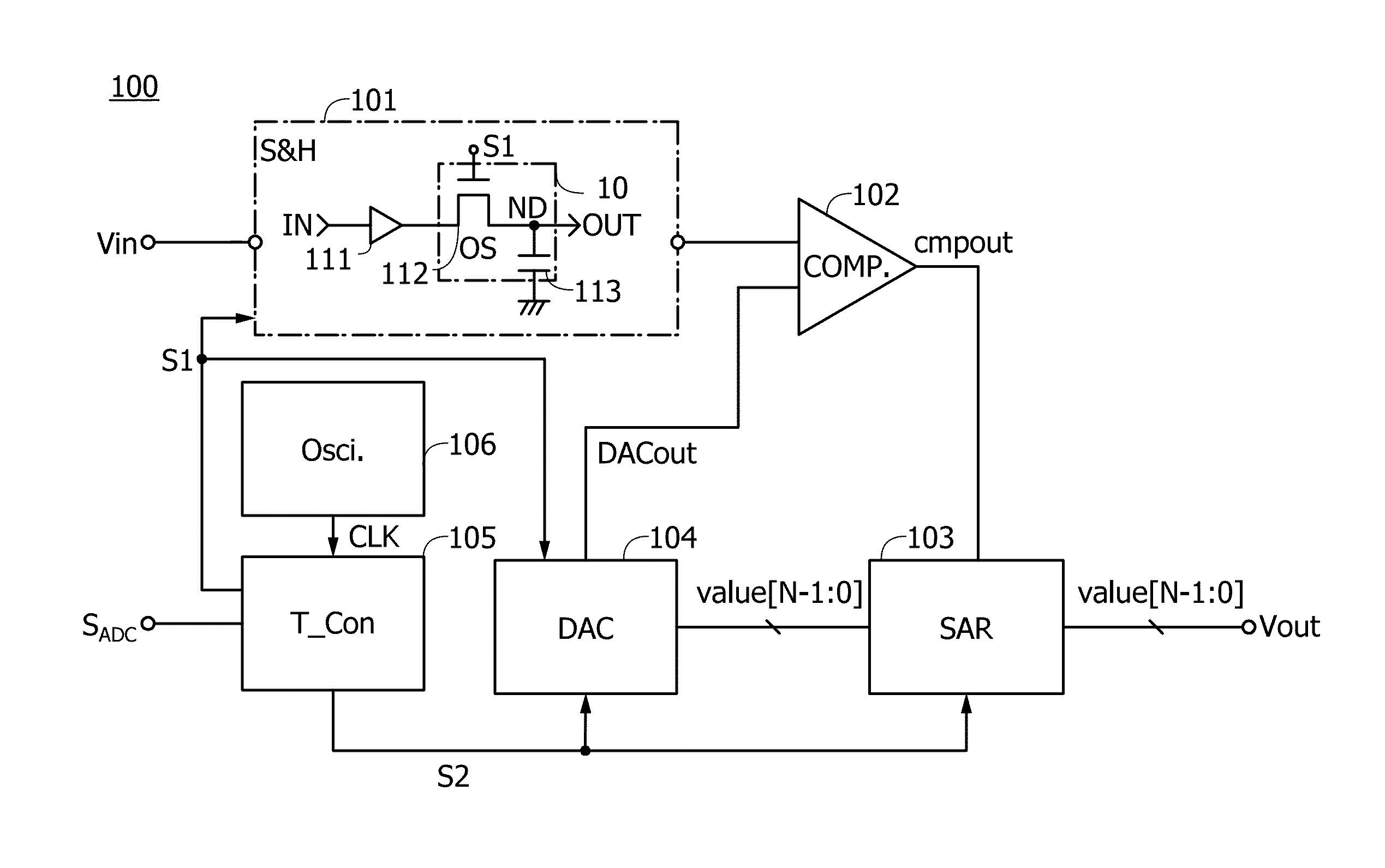
[0079]A structure of a semiconductor device of one embodiment of the present invention is described with reference to FIG. 1.

[0080]In this specification and the like, a semiconductor device generally means a device that has semiconductor characteristics. Furthermore, a semiconductor device sometimes means a circuit utilizing semiconductor characteristics or the whole of a system including the circuit.

[0081]FIG. 1 is a block diagram illustrating the structure of a semiconductor device in one embodiment of the present invention.

[0082]A semiconductor device 100 includes a sample-and-hold circuit 101 (denoted by S&H in the drawing), a comparator 102 (denoted by COMP in the drawing), a successive approximation register 103 (denoted by SAR in the drawing), a digital-analog converter circuit 104 (also referred to as a DA converter, and denoted by DAC in the drawing), a timing controller 105 (denoted by T_Con in the drawing), and an oscillator circuit 106 (denoted by Osci. in the drawing).

[...

embodiment 2

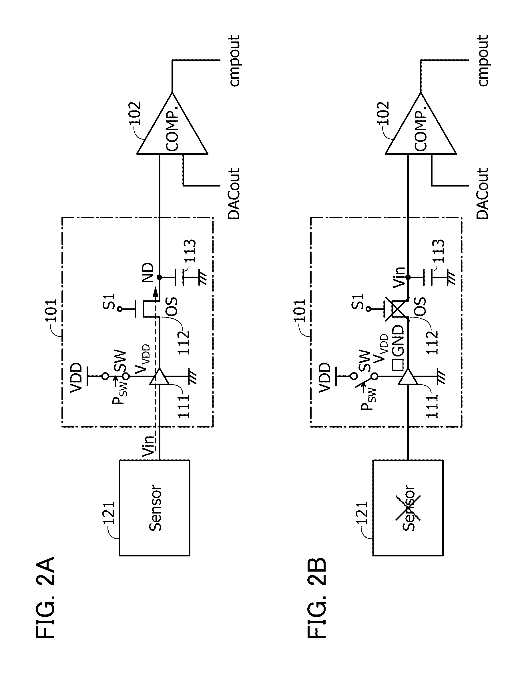
[0130]In this embodiment, a circuit structure and an operation different from those of the semiconductor device shown in Embodiment 1 will be described.

[0131]A semiconductor device 200 shown in FIG. 10 includes the sample-and-hold circuit 101, the successive approximation register 103, the digital-analog converter circuit 104, the timing controller 105, and the oscillator circuit 106.

[0132]The semiconductor device 200 of FIG. 10 is different from the semiconductor device of FIG. 1 in that the digital-analog converter circuit 104 includes a transistor 211 and a capacitor 212 for holding digital data. A gate of the transistor 211 is supplied with a control signal S3value[N-1:0] corresponding to each bit for controlling the on / off state from the timing controller 105. In this embodiment, different points from Embodiment 1 are described in detail, and a repeated explanation will be omitted.

[0133]When the transistor 211 is turned off, a charge corresponding to the potential of digital da...

embodiment 3

[0154]In this embodiment, as an application example of the semiconductor devices each functioning as an AD converter described in Embodiments 1 and 2, a wireless sensor will be described. Note that a wireless sensor is referred to as a radio frequency (RF) sensor or the like.

[0155]The wireless sensor receives a wireless signal from a wireless communication device and outputs data obtained in a sensor circuit to the wireless communication device. Note that any wireless communication device is acceptable as long as it can transmit and receive a wireless signal; for example, an interrogator, a smart meter, a mobile phone, a personal computer, or a wireless terminal that collects data can be used.

[0156]The wireless sensor is preferably a passive wireless sensor that operates with a received wireless signal used as power. The passive wireless sensor does not include a secondary battery, which leads to miniaturization and increase in the degree of arrangement freedom. Note that it may inc...


PUM


Abstract

An object is to reduce power consumption of an analog-digital converter circuit. An analog potential obtained in a sensor or the like is held in a sample-and-hold circuit including a transistor with an extremely low off-state current. In the sample-and-hold circuit, the analog potential is held in a node which is able to hold a charge by turning off the transistor. Then, power supply to a buffer circuit or the like included in the sample-and-hold circuit is stopped to reduce power consumption. In a structure where a potential is held in each node, power consumption can be further reduced when a transistor with an extremely low off-state current is connected to a node holding a potential of a comparator, a successive approximation register, a digital-analog converter circuit, or the like, and power supply to these circuits is stopped.

Description

BACKGROUND OF THE INVENTION[0001]1. Field of the Invention[0002]One embodiment of the present invention relates to a semiconductor device, a wireless sensor, and an electronic device.[0003]Note that one embodiment of the present invention is not limited to the above technical field. The technical field of the invention disclosed in this specification and the like relates to an object, a method, or a manufacturing method. In addition, one embodiment of the present invention relates to a process, a machine, manufacture, or a composition of matter. Specific examples of the technical field of one embodiment of the present invention disclosed in this specification include a semiconductor device, a display device, a light-emitting device, a power storage device, an imaging device, a memory device, a method for driving any of them, and a method for manufacturing any of them.[0004]2. Description of the Related Art[0005]An analog-digital converter circuit (hereinafter referred to as an AD co...

Claims


Application Information

Patent Timeline
Patent Type & Authority Applications(United States)
IPC IPC(8): H03M1/00H03M1/12H03M1/38
CPCH03M1/002H03M1/124H03M1/38H03M1/1245H03M1/466G11C27/02
Inventor SHIONOIRI, YUTAKAKATO, KIYOSHIATSUMI, TOMOAKI
Owner SEMICON ENERGY LAB CO LTD
Why Eureka
Try Eureka