Field-shielded SOI-MOS structure free from floating body effect, and method of fabrication therefor

a soi-mos and field shielding technology, applied in the field of field shielded soi-mos structure and free from floating body effect, can solve the problems of floating body potential of nmosfet-soi devices, unstable stability, and inability to be widely accepted by system and circuit design communities, and achieve enhanced recombination centers, enhanced recombination carriers, and reduced recombination time constant

Inactive Publication Date: 2005-08-23
MICRON TECH INC
View PDF1 Cites 30 Cited by
  • Summary
  • Abstract
  • Description
  • Claims
  • Application Information

AI Technical Summary

Benefits of technology

[0012]The present invention provides a silicon-on-insulator structure free from floating body effects, and a method of fabrication therefor. More specifically, the present invention provides a structure capable of facilitating the enhanced recombination of charge carriers, which results in a greatly reduced recombination time constant.
[0013]Accordingly, the present invention relates to a structure having a field shield integration configuration that provides an effective drift field for holes and simultaneously enhanced recombination centers for positive-charge carriers (holes) and negative-charge carriers (electrons). The effective drift field and the enhanced recombination centers facilitate the rapid recombination of the charge carriers, leading to a very small recombination time constant. The structure comprises a silicon substrate, an oxide insulation layer disposed above the silicon substrate, a silicon body layer disposed above the oxide insulation layer, and a field shield gate disposed above the silicon body layer. The field shield gate includes a conductor portion, and an alumina insulation layer disposed beneath the conductor portion. The oxide insulation layer and the silicon body layer each include at least one channel stop region, and at least one recombination center for the recombination of positive- and negative-charge carriers.
[0014]The present invention also relates to a method of fabricating the above-described silicon-on-ins

Problems solved by technology

SOI-CMOS technology, however, has yet to be widely accepted by the systems and circuit design communities because of the complexity of managing an anomalous effect termed the “floating body effect” (hereinafter “FBE”), of the SOI devices, and in particular, of NFET-SOI devices.
Unlike bulk NMOSFET devices, in which the body is tied to either a fixed potential or to the source of the device, body potential in NMOSFET-SOI devices is floating, and remains unstable due to the complex dynamics of both positive-charge carrier, or “hole,” generation by impact ionization at the drain edge, and by recombination and diffusion.
As a result of this floating potential, NMOSFET-SOI devices exhibit several undesirable characteristics, such as a “kink effect” (current enhancement) in the Id-Vg characteristics of the device, enhanced leakage attributable to parasitic (npn

Method used


Image

  • Field-shielded SOI-MOS structure free from floating body effect, and method of fabrication therefor
  • Field-shielded SOI-MOS structure free from floating body effect, and method of fabrication therefor
  • Field-shielded SOI-MOS structure free from floating body effect, and method of fabrication therefor

Examples


embodiment 200

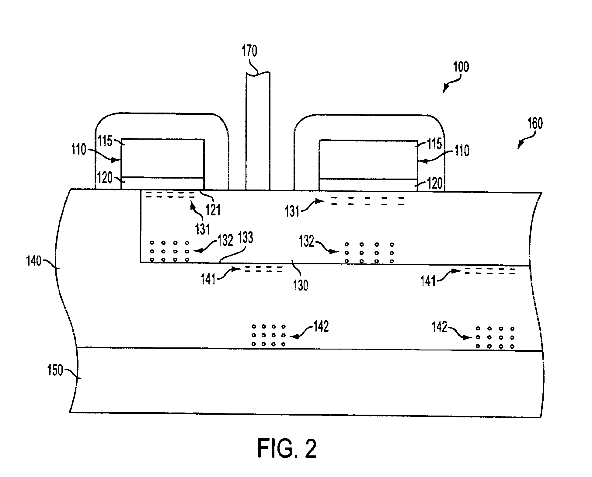
[0037]FIG. 3 is a partial cross-sectional view of an SOI-NFET active device embodiment 200 of the structure 100 depicted in FIG. 2. In addition to the features depicted in FIG. 2, active device 200 includes an NFET active layer 210 of n+ polysilicon and active device gate 215. As indicated above, the drift field generated by the negative charges near the interface 121 attracts holes, such as those schematically depicted beneath the active device gate 215, which are then recombined at the recombination center 132.

embodiment 300

[0038]FIG. 4 is a plan view of the layout of an SOI-NMOSFET active device embodiment 300 of the structure depicted in FIG. 2. FIG. 5 is a partial cross-sectional view through the channel of the layout depicted in FIG. 4. In addition to the features depicted in FIG. 2, active device 300, which provides shallow trench isolation, includes active gate 310; active gate contact 311; n+source 320; source contact 340; n+ drain 330; drain contact 350, and body contact 131.

embodiment 400

[0039]FIG. 6 is a partial cross-sectional view of an SOI-CMOS active device embodiment 400 of the structure depicted in FIG. 2. In addition to the features depicted in FIG. 2, active device 400, which also provides shallow trench isolation, includes a silicon body layer 410 of a second conductivity type, such as an n-type, the silicon body layer 410 having a channel stop region 411 and a recombination center 412; an n-body contact 420; an NFET active device 430; and a PFET active device 440.

[0040]A chip produced from the structure 100 (or any of the above-described various embodiments thereof depicted in FIGS. 3-6) may be incorporated in any fabricated semiconductor device, including various processor system components, such as for example, a central processing unit (CPU) or in any of the various types of memory devices, such as for example, RAM, ROM, and others. It may also be used in any type of integrated circuit controller for a floppy disk, a hard disk, a ZIP, or a CD-ROM disk....


PUM


Abstract

A silicon-on-insulator structure provides an effective drift field for holes, and simultaneously enhanced recombination centers for holes and electrons. The structure includes a silicon substrate, an oxide insulation layer disposed above the silicon substrate, a silicon body layer disposed above the oxide insulation layer, and a field shield gate disposed above the silicon body layer. The field shield gate includes a conductor portion, and an alumina insulation layer disposed beneath the conductor portion. The oxide insulation layer and the silicon body layer each include at least one channel stop region, and at least one recombination center for the recombination of positive- and negative-charge carriers. The effective drift field and enhanced recombination centers facilitate the rapid recombination of the charge carriers, leading to a very small recombination time constant, which overcomes the floating body effect associated with conventional silicon-on-insulator structures.

Description

BACKGROUND OF THE INVENTION[0001]1. Field of the Invention[0002]This invention relates generally to the field of semiconductor memory and logic devices. The invention relates more specifically to a silicon-on-insulator structure, and a method of fabrication therefor.[0003]2. Description of the Related Art[0004]In the field of microelectronics, SOI (Silicon-on-Insulator)-CMOS technology has been demonstrated to have significant speed, power, and radiation immunity advantages over bulk CMOS technology. See, e.g., “Scalability of SOI Technology into 0.13 um 1.2 V CMOS Generation,” E. Leobandung, et al., IEDM, 1998, pp. 403-406, and “SOI and Device Scaling,” C. Hu, Proceedings of IEEE International SOI Conference, Oct. 1998, pp. 1-4.[0005]SOI-CMOS technology, however, has yet to be widely accepted by the systems and circuit design communities because of the complexity of managing an anomalous effect termed the “floating body effect” (hereinafter “FBE”), of the SOI devices, and in partic...

Claims


Application Information

Patent Timeline
IPC IPC(8): H01L21/70H01L27/12H01L21/84
CPCH01L21/84H01L27/1203
Inventor BHATTACHARYYA, ARUP
Owner MICRON TECH INC
Why Eureka
Try Eureka