Light-emitting device with head-to-tail P-type and N-type transistors

a technology of light-emitting devices and transistors, applied in the field of microelectronic devices, can solve the problems of limited efficiency of recombining charge carriers

Active Publication Date: 2014-05-20
COMMISSARIAT A LENERGIE ATOMIQUE ET AUX ENERGIES ALTERNATIVES
View PDF3 Cites 0 Cited by
  • Summary
  • Abstract
  • Description
  • Claims
  • Application Information

AI Technical Summary

Benefits of technology

[0014]According to the invention, the flows of electrons and holes can be adjusted independently by the manner in which the first said transistor and the second said transistor are biased. To increase the mobility of the holes in the device it is, for example, possible to increase the current generated in the channel of the second transistor. The number of recombinations of electron / hole pairs is increased by this means.
[0015]Such a device is compact, while enabling a light flow to be obtained which can vary over a broad range.
[0019]It is thus possible to implement a first flow of a first type of charge carriers, for example of holes flowing in said given region, and a second flow of charge carriers of a second type flowing in said given region, in the same direction as that of the first flow.
[0020]This can enable the recombinations between charge carriers to be improved.
[0027]Implementation of the given region using such a material can enable improved efficiency to be obtained in terms of photoemission.
[0029]This can enable improved confinement of the carriers in the given region to be obtained. It can also enable the carriers to be located in a region where the recombinations will take place.

Problems solved by technology

Such a device poses problems of encumbrance, and is also of limited efficiency for recombining the charge carriers.

Method used


Image

  • Light-emitting device with head-to-tail P-type and N-type transistors
  • Light-emitting device with head-to-tail P-type and N-type transistors
  • Light-emitting device with head-to-tail P-type and N-type transistors

Examples


Embodiment Construction

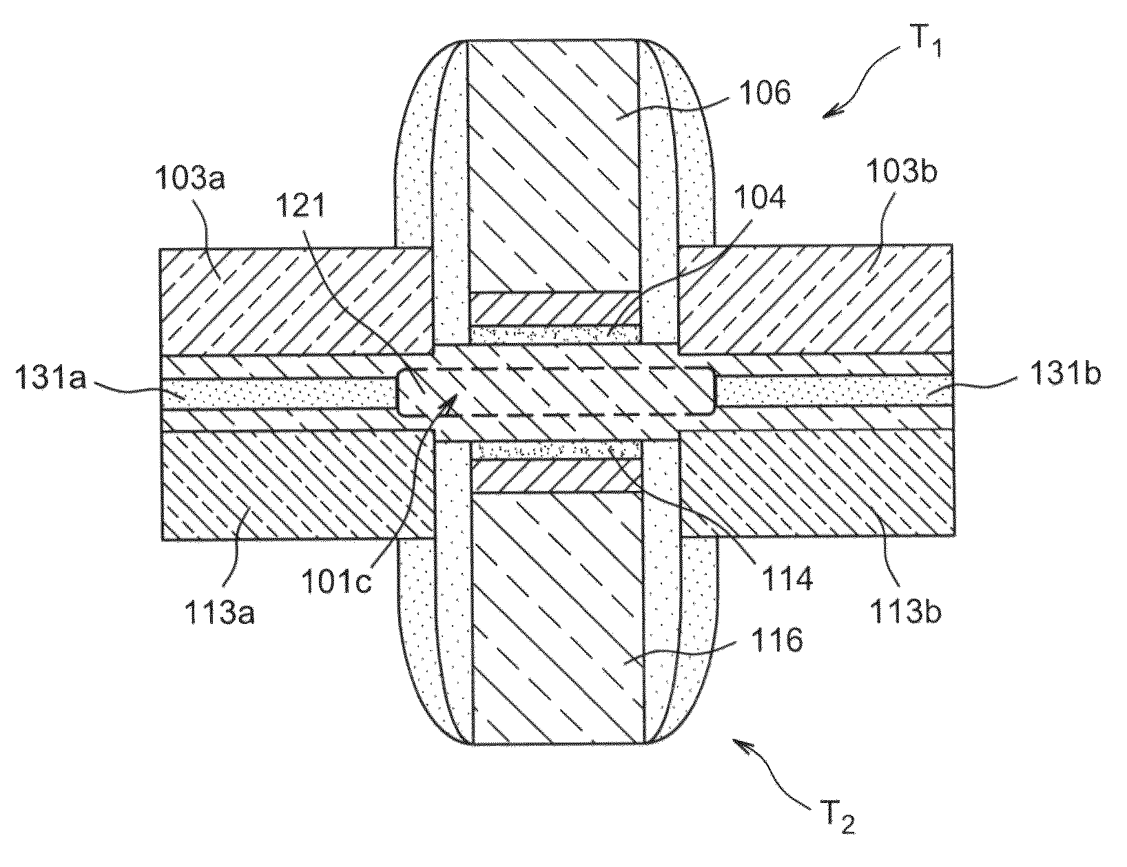
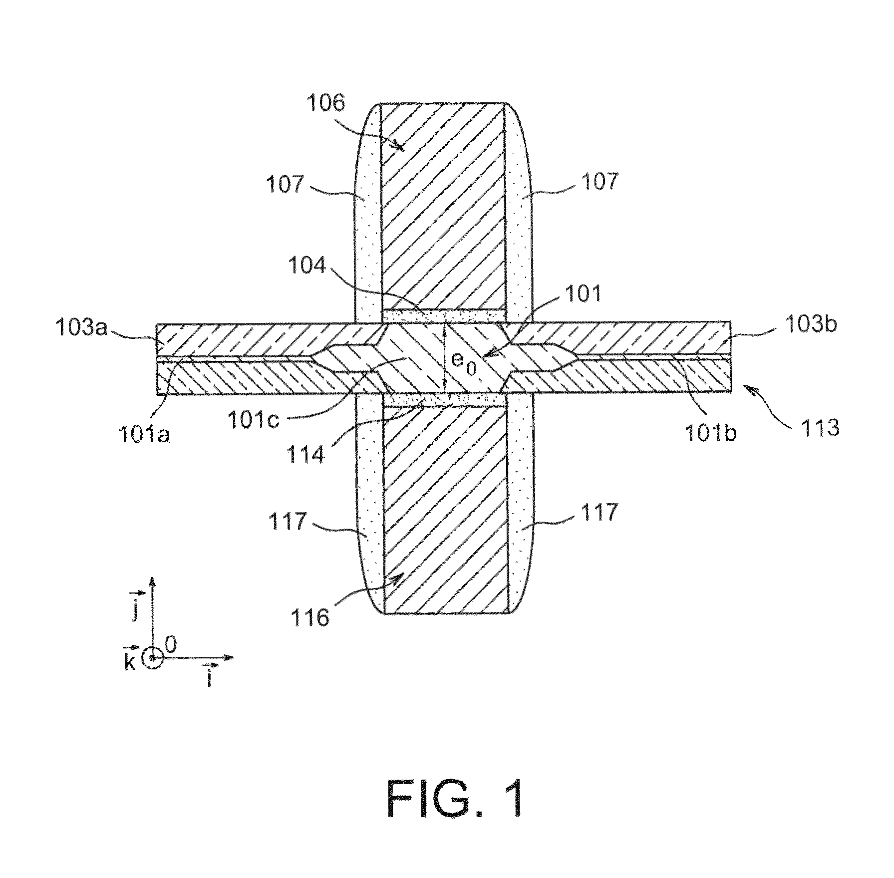
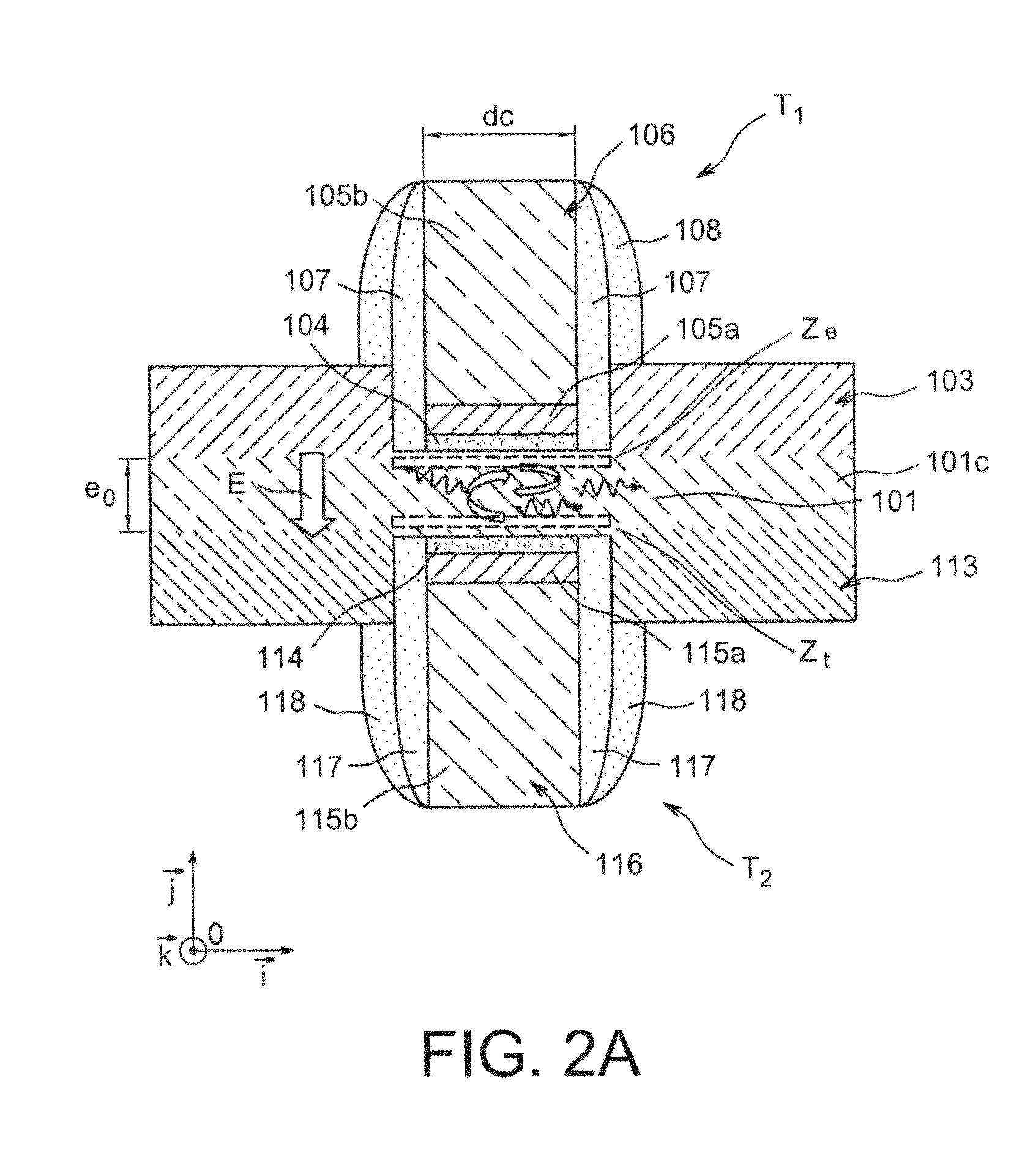
[0011]The present invention relates to a microelectronic light-emitting device including at least one first transistor having source and drain regions formed in at least one first doped semiconductor N region and one gate, at least one second transistor having source and drain regions formed in at least one second doped semiconductor P region and one gate, where the gate of the first transistor and the gate of the second transistor are positioned opposite one another, either side of a region including a given region made of at least one intrinsic and / or undoped semiconductor material.

[0012]Such a device enables a current of holes and a current of electrons to be adjusted independently.

[0013]In a semiconductor region the electrons and the holes generally do not have the same ability to move or the same mobility. In a light-emitting diode only a single current flows, and the electron flow is therefore equal to the flow of holes. The latter, which generally move slowly, can limit the r...


PUM


Abstract

A light-emitting microelectronic device including a first N-type transistor (T1) and a second P-type transistor (T2), the respective gates of which are formed opposite one another, either side of an intrinsic semiconductor material region.

Description

TECHNICAL FIELD[0001]The present invention relates to the field of microelectronics and, more specifically, light-emitting microelectronic devices.[0002]It concerns a light-emitting device enabling a luminous flux to be obtained which can vary over a broad range, whilst having an improved design in particular in terms of encumbrance.PRIOR ART[0003]It is well known to produce light-emitting diodes formed, for example, from a P-N junction or a P-I-N junction.[0004]In such devices, electron-hole pairs are recombined in a region called a “space charge region”, so as to create photons. Hetero-structures with quantum wells can be present in the space charge region, in order to increase recombination efficiency.[0005]A quantum well can be produced using a stack of layers made of semiconductor materials with different gaps, including for example a layer made of a material with a small gap positioned between two layers of material with a larger gap.[0006]Light-emitting transistors also exist...

Claims


Application Information

Patent Timeline
Patent Type & Authority Patents(United States)
IPC IPC(8): H01L33/00
CPCH01L33/0079H01L27/153H01L33/0041H01L33/0093
Inventor GRENOUILLET, LAURENTVINET, MAUD
Owner COMMISSARIAT A LENERGIE ATOMIQUE ET AUX ENERGIES ALTERNATIVES
Why Eureka
Try Eureka