CMOS-compatible germanium tunable laser

Active Publication Date: 2018-05-29
IHP GMBH INNOVATIONS FOR HIGH PERFORMANCE MICROELECTRONICS LEIBNIZ INST FUR INNOVATIVE
View PDF33 Cites 0 Cited by
  • Summary
  • Abstract
  • Description
  • Claims
  • Application Information

AI Technical Summary

Benefits of technology

[0019]As a consequence of the tensile strain, the electronic energy bands are modified in a way that the radiative recombination of electron-hole pairs is enhanced in comparison to the Ge bulk case. Moreover, the energy-band gap is shrunk in comparison with that of unstrained Ge. As a consequence, the light emission efficiency of the material is increased, with the emission occurring at a wavelength increasing with the amount of tensile strain.
[0020]As will be disclosed in the context of the description of preferred embodiments, the light emitter device of the present invention forms an advantageous device platform that allows adding tuning elements, which enable a tuning of the emitted wavelength by strain adjustment, either fixed via proper selection of the stressor material, or even variable under operation of the device via an electrical control.
[0033]The spatial separation of the high doping areas and the light emission area brings about key advantages. These include a low free-carrier absorption and a low Auger recombination. Furthermore, due to a lowering of the conduction band minimum and an increase of the valence band maximum in energy under tensile strain, electrons as well as holes will drift to the highly strained intrinsic part and, due to this local confinement by band gap engineering, be available for efficient direct recombination and light output.
[0036]Such a high level of strain allows reaching a net gain value as high as 2000 cm−1 with doping levels even below 2×1019 cm−3, for instance as low as 8×1018 cm−3. This is a much easier-to-achieve donor density. This preferred decrease of the requested donor density in the present embodiment has another beneficial effect. As a matter of fact, below the of 2×1019 cm−3 limit, the gain is expected to increase with the operating temperature with a gain maximum achieved at 350 K, i.e., at a temperature very close to the on-chip temperature in standard CMOS devices.
[0037]Nonetheless, other, in particular higher doping levels can be used in other embodiments to partially compensate the strain-induced band gap shrinkage to maximize the optical gain at a desired emission wavelength.
[0052]This CMOS-compatible processing enables a cost-efficient fabrication of the light emitter device in large volumes in the context of standard processing techniques.

Problems solved by technology

However the maximum reported gain for highly doped, thermal tensile strained structures is 50 cm−1, owing to the difficulties in to real high- and ultra-high n-doping in Ge due to donor solubility, dopant activation, and material processing.

Method used


Image

  • CMOS-compatible germanium tunable laser
  • CMOS-compatible germanium tunable laser
  • CMOS-compatible germanium tunable laser

Examples


Embodiment Construction

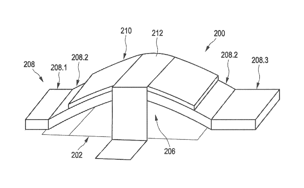
[0057]FIG. 1 shows a schematic cross sectional view of an embodiment of a light emitter device 100. The graphical representation of FIG. 1 is simplified in that only a lateral section of the device is shown. However, since the device is symmetrical, the parts not shown do not contain structural features differing from those shown in the Figure. The symmetry is of mirror type, and the position of the mirror plane M, which extends perpendicularly to the cross-sectional plane of FIG. 1, is indicated at the right edge of FIG. 1. Horizontal dotted lines at the left and right edges of the layer structure are provided to more clearly show the respective position and thickness of the individual layers in layer structure of the light emitter device 100. A further simplification of the graphical representation in FIG. 1 is that only structural elements are shown, which are essential to understand the structure of the present embodiment. In particular, no contact structures are shown.

[0058]In ...


PUM


Abstract

A semiconductor light emitter device, comprising a substrate, an active layer made of Germanium, which is configured to emit light under application of an operating voltage to the semiconductor light emitter device, wherein a gap is arranged on the substrate, which extends between two bridgeposts laterally spaced from each other, the active layer is arranged on the bridgeposts and bridges the gap, and wherein the semiconductor light emitter device comprises a stressor layer, which induces a tensile strain in the active layer above the gap.

Description

CROSS REFERENCE TO RELATED APPLICATIONS[0001]This application is the U.S. National Stage of International Application Number PCT / EP2013 / 052702 filed on Feb. 11, 2013 which application claims priority under 35 USC § 119 to European Patent Application No. 12154997.6 filed on Feb. 10, 2012. Both applications are hereby incorporated by reference in their entirety.TECHNICAL FIELD[0002]The present invention relates to semiconductor light emitter devices, in particular, a CMOS-compatible light emitter device.BACKGROUND OF THE INVENTION[0003]An efficient electrically-pumped light emitter integrated in the standard CMOS technology has been so far the Holy Grail of the monolithic electronic-photonic integration. As a matter of fact, rapid advances in Si photonics over the last decade have enabled mass production of higher-functionality and lower-cost photonic integrated circuits, in which all the active and passive components such as waveguides, couplers, modulators, photodetectors, etc., exc...

Claims


Application Information

Patent Timeline
Patent Type & Authority Patents(United States)
IPC IPC(8): H01L27/15H01L21/00H01S5/32H01S5/02H01L33/34H01L31/12
CPCH01S5/3201H01S5/3223H01S5/021H01L33/34
Inventor CAPELLINI, GIOVANNIWENGER, CHRISTIANSCHRODER, THOMASKOZLOWSKI, GRZEGORZ
Owner IHP GMBH INNOVATIONS FOR HIGH PERFORMANCE MICROELECTRONICS LEIBNIZ INST FUR INNOVATIVE
Why Eureka
Try Eureka