Method of making a test structure for gate-body current and direct extraction of physical gate length using conventional CMOS

a test structure and gate-body current technology, applied in the direction of individual semiconductor device testing, semiconductor/solid-state device testing/measurement, instruments, etc., can solve the problems of loss of gate control of transistor current, kink in transistor current/voltage curve, and carrier multiplication near the drain end of the channel

Inactive Publication Date: 2006-07-04
GLOBALFOUNDRIES INC
View PDF7 Cites 30 Cited by
  • Summary
  • Abstract
  • Description
  • Claims
  • Application Information

AI Technical Summary

Benefits of technology

The invention describes methods for making computer chips with built-in testing structures that can be produced efficiently during chip fabrication. This allows for better quality control over semiconductor devices used in these computers.

Problems solved by technology

The technical problem addressed in this patent text relates to the development of a method for accurately measuring the important parameters of metal oxide semiconductor (MOS) transistors, particularly the gate-body current and physical gate length. Current methods require a connected body when measuring these quantities, leading to significant errors caused by the introduced extra current. There is a need for a more reliable testing technique to ensure accuracy in evaluating MOS transistor performance.

Method used


Image

  • Method of making a test structure for gate-body current and direct extraction of physical gate length using conventional CMOS
  • Method of making a test structure for gate-body current and direct extraction of physical gate length using conventional CMOS
  • Method of making a test structure for gate-body current and direct extraction of physical gate length using conventional CMOS

Examples


Embodiment Construction

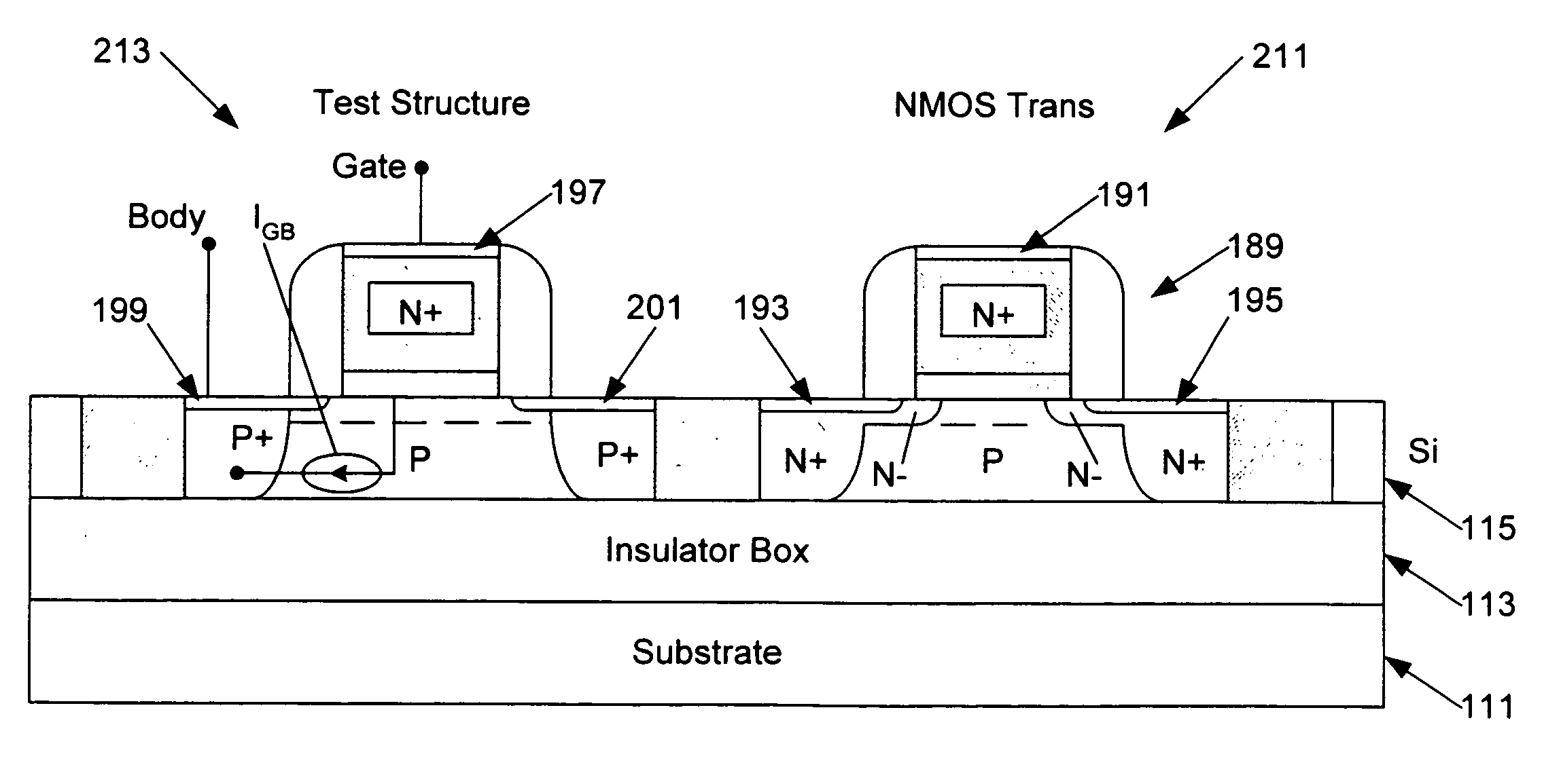
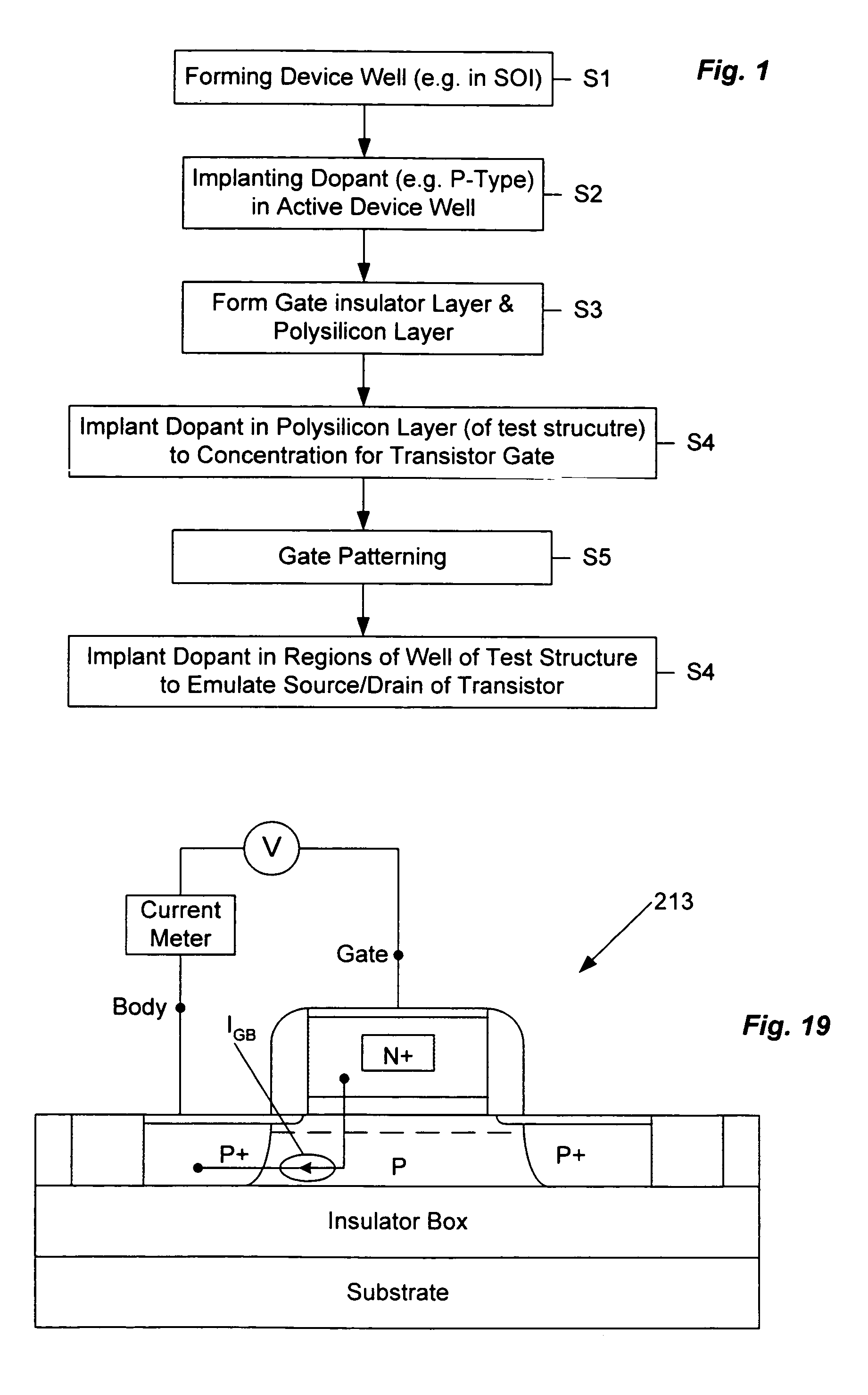
[0041]The various techniques disclosed herein relate to semiconductor processing to construct a test structure, which is useful in measuring gate-body currents in MOS transistor devices and / or in measurement of gate current as a means to measure physical gate length of a transistor device. The test structure is designed to mimic an MOS device of interest for testing and analysis purposes, so that tests on the test structure provide desired information regarding the MOS device of interest. The MOS device and the test structure may be elements constructed on a bulk semiconductor substrate, however, the methodology and the test structure are particularly advantageous when applied in the context of silicon-on-insulator (SOI) type integrated circuits.

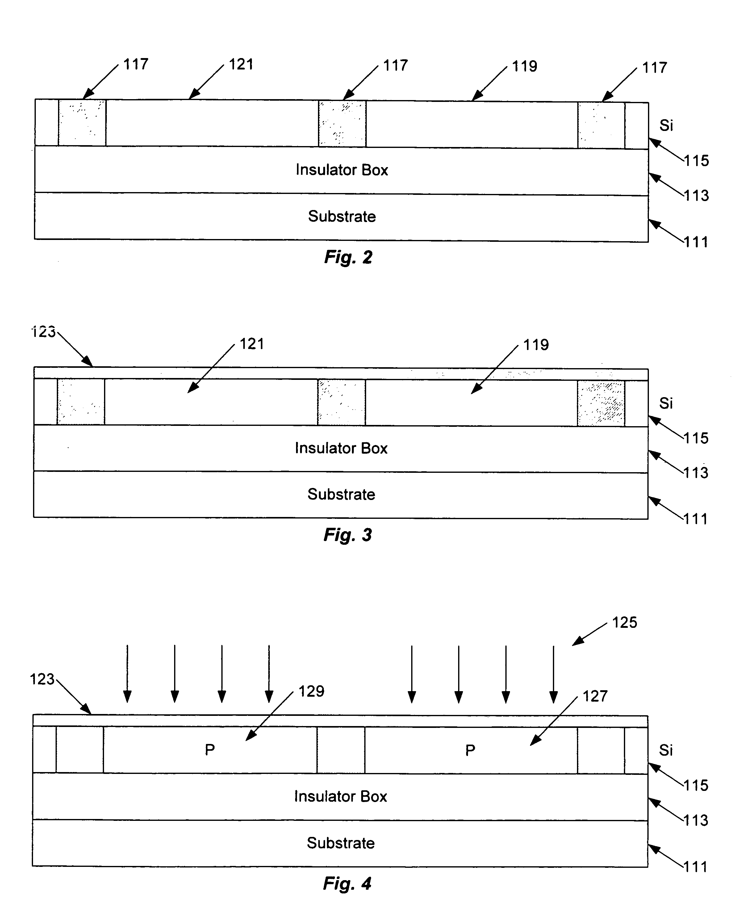
[0042]Since the techniques of particular interest at this point relate to manufacture of the test structure, an exemplary manufacturing process is described, first at a high level with regard to FIG. 1 and then in more detail with reference ...


PUM


Abstract

A structure for testing relative to an MOS transistor, can be easily constructed as part of the CMOS process flow. A doped device well is formed, for example, in a silicon-on-insulator structure. The concentration level in the well corresponds to that for a well of the transistor. Gate insulator and polysilicon layers are formed, and the polysilicon is implanted with dopant, to a concentration level expected in the transistor gate. After gate patterning, the methodology involves forming sidewall spacers and implanting dopant into the active device well, to form regions in the test structure corresponding to the transistor source and drain. Although the concentrations mimic those in the transistor source and drain, these test structure regions are doped with opposite type dopant material. The test structure enables accurate measurement of the gate-body current, for modeling floating body effects and/or for measurement of gate length.

Description


Claims


Application Information

Patent Timeline
Owner GLOBALFOUNDRIES INC
Why Eureka
Try Eureka