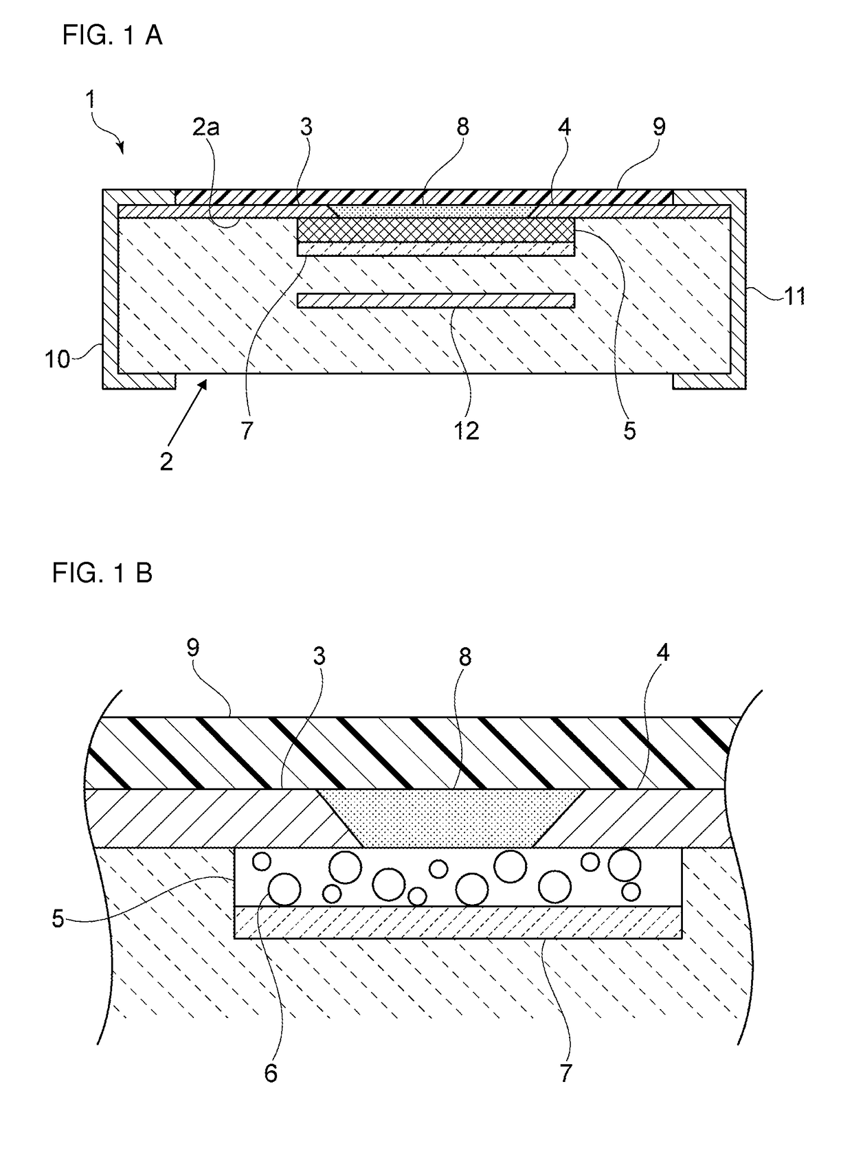
ESD protection device
a protection device and shielding technology, applied in the direction of emergency protective arrangements for limiting excess voltage/current, spark gap details, circuit arrangements, etc., can solve the problems of difficult to make its discharge inception voltage sufficiently low, and insufficient discharge inception voltage. achieve the effect of low discharge inception voltag
- Summary
- Abstract
- Description
- Claims
- Application Information
AI Technical Summary
Benefits of technology
Problems solved by technology
Method used
Image


Examples
examples 3 and 4
[0116]An electrode paste having the same composition as the discharge electrode paste used in Example 2 was prepared as back electrode paste.
[0117]The back electrode paste was applied to a mother ceramic green sheet using screen printing in such a manner that it would be isolated from outer electrodes. ESD protection devices of Example 3 were obtained in the same way as in Example 1, except that this mother ceramic green sheet carrying the back electrode paste was inserted.
[0118]ESD protection devices of Example 4 were then obtained in the same way as in Example 1, except that the back electrode was applied in such a manner that it would finally be coupled with an outer electrode.
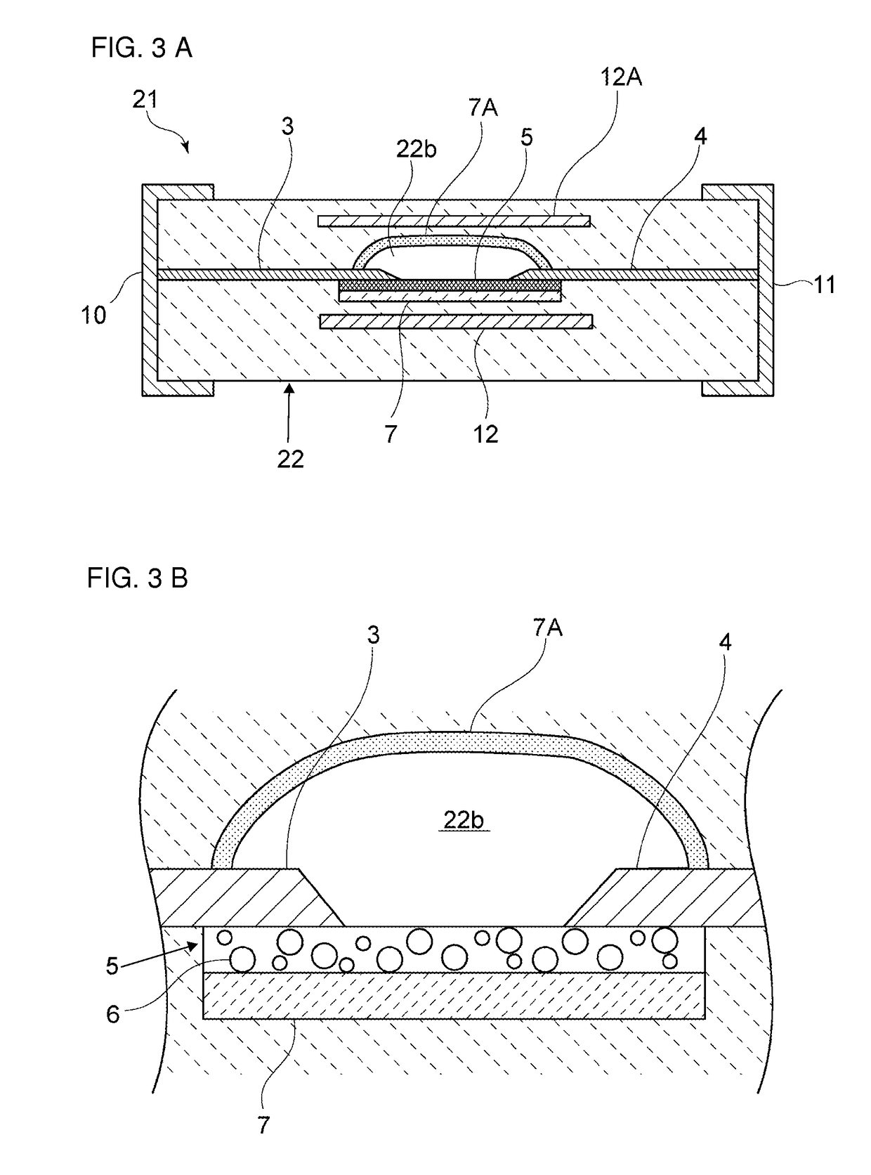
[0119]In Examples 3 and 4, the back electrode was located 10 μm lower than the positions where the first and second discharge electrodes 3 and 4 would be in the mother multilayer body.
[0120]The percentage normal operation of the ESD protection devices of Examples 3 and 4 obtained in this way was evaluated i...
PUM
 Abstract
Description
Claims
Application Information