LED flip-chip package substrate and LED package structure
a flip-chip package and substrate technology, applied in the field of led packaging, can solve the problems of poor heat conductivity, poor electrical insulation and stability, poor electrical insulation thereof, etc., and achieve the effects of high heat conductivity, high reflectivity, and high stability
- Summary
- Abstract
- Description
- Claims
- Application Information
AI Technical Summary
Benefits of technology
Problems solved by technology
Method used
Image

Examples
first embodiment
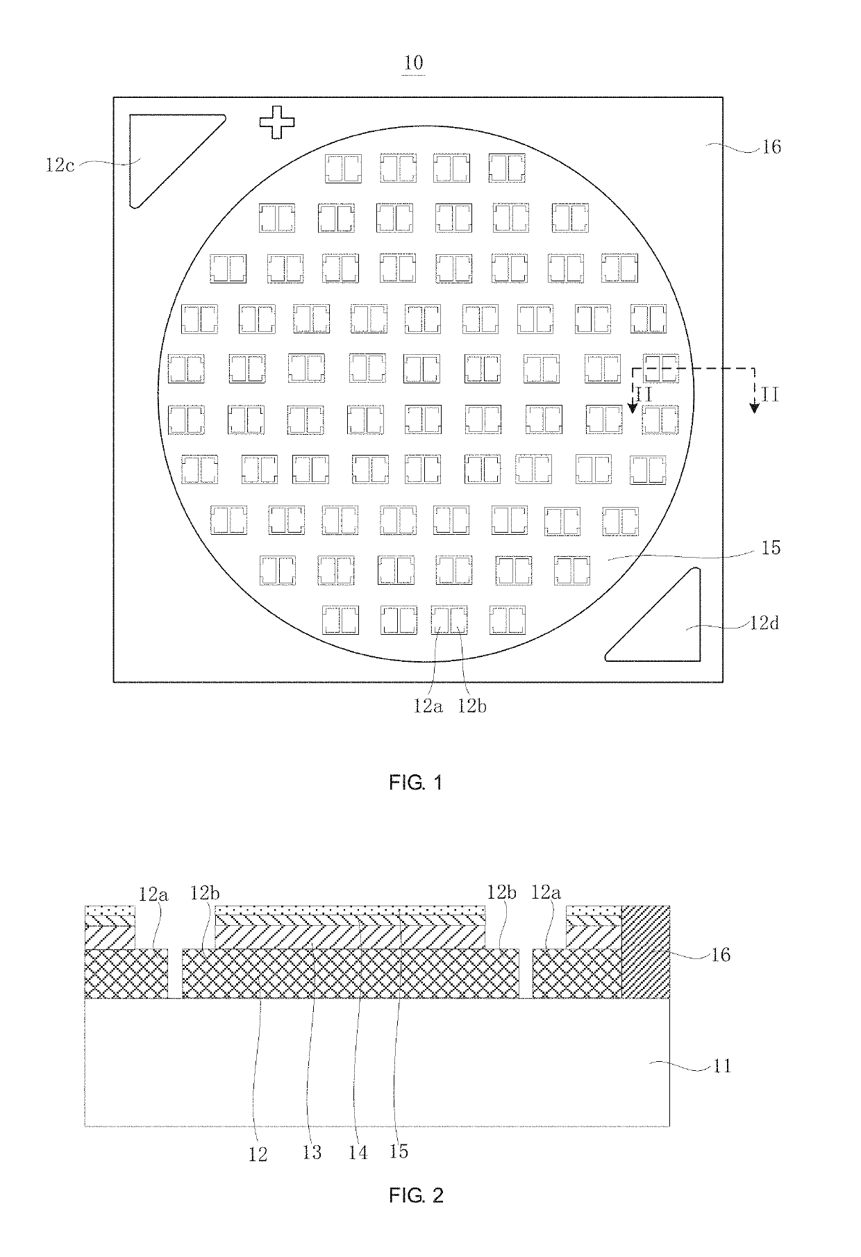
[0032]Referring to FIG. 1 and FIG. 2, FIG. 1 is a top schematic view of a LED flip-chip package substrate according to a first embodiment of the disclosure. FIG. 2 is an enlarged local schematic view of a cross-sectional structure of the LED flip-chip package substrate shown in FIG. 1 taken along a line of II-II. A LED flip-chip package substrate 10 of the embodiment includes a ceramic base 11, a conductive wire layer 12, an insulating protective layer 13, a metallic reflective layer 14, an optical anti-reflective film 15 and an ink layer 16.
[0033]The ceramic base 11 is preferably an aluminum nitride (AlN) ceramic base. The AlN ceramic base has high heat conductivity (200 W / m·K), superior insulation (volume resistivity>1013 Ω·cm) as well as high chemical and thermal stability. The conductive wire layer 12 is disposed on the ceramic base 11. The conductive wire layer 12 includes multiple (i.e., more than one) pairs of pads 12a and 12b, and a positive electrode 12c and a negative elec...
second embodiment
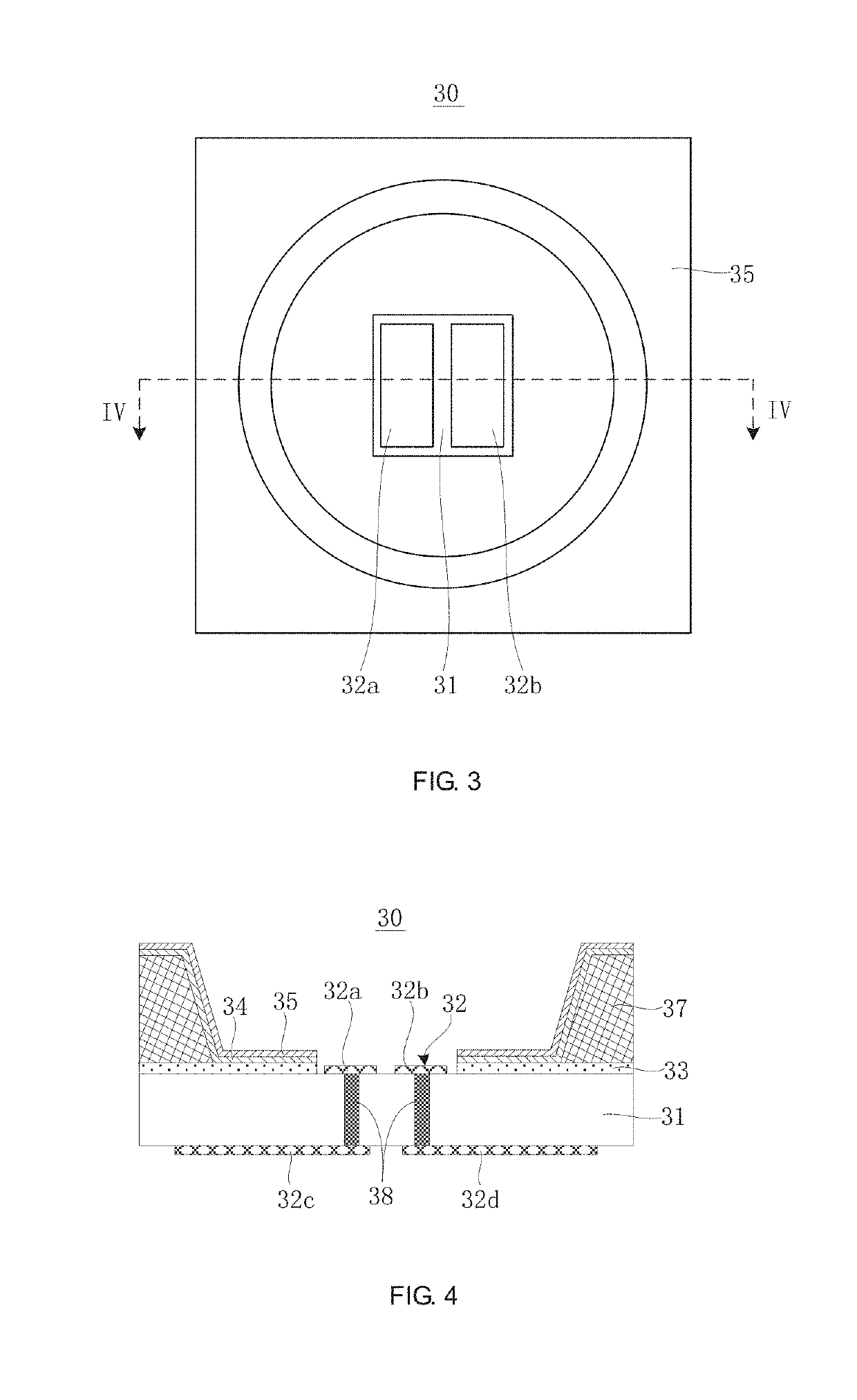
[0035]Referring to FIG. 3 and FIG. 4, FIG. 3 is a top schematic view of a LED flip-chip package substrate according to a second embodiment of the disclosure. FIG. 4 is a cross-sectional schematic view of the LED flip-chip package substrate shown in FIG. 3 taken along a line of IV-IV. The LED flip-chip package substrate 30 of the embodiment includes a ceramic base 31, a conductive wire layer 32, an insulating protective layer 33, a metallic reflective layer 34, an optical anti-reflective film 35 and a reflective cup 37.
[0036]The ceramic base 31 is preferably an aluminum nitride (AlN) ceramic base. The AlN ceramic base has high heat conductivity (200 W / m·K), superior insulation (volume resistivity>1013 Ω·cm) as well as chemical and thermal stability. The conductive wire layer 32 is formed on the ceramic base 31 by for example a thick film process or a thin film process, which can be a silver (Ag) layer produced by the thick film process (e.g., sintering), or a copper (Cu) / nickel (Ni) / ...
third embodiment
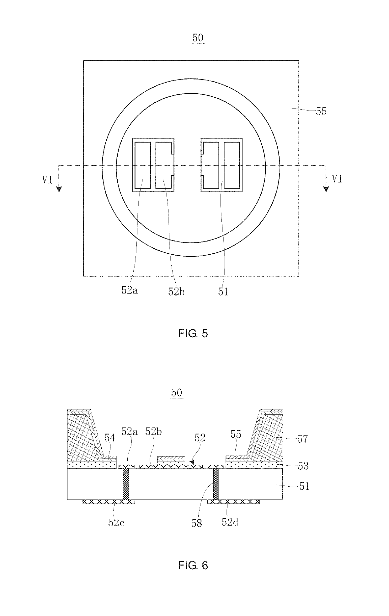
[0037]Referring to FIG. 5 and FIG. 6, FIG. 5 is a top schematic view of a LED flip-chip package substrate according to a third embodiment of the disclosure. FIG. 6 is a cross-sectional schematic view of the LED flip-chip package substrate shown in FIG. 5 taken along a line of VI-VI. The LED flip-chip package substrate 50 of the embodiment includes a ceramic base 51, a conductive wire layer 52, an insulating protective layer 53, a metallic reflective layer 54, an optical anti-reflective film 55 and a reflective cup 57.
[0038]The ceramic base 51 is preferably the aluminum nitride (AlN) ceramic base. The AlN ceramic base has high heat conductivity (200 W / m·K), superior insulation (volume resistivity>1013 Ω·cm) as well as chemical and thermal stability. The conductive wire layer 52 is formed on the ceramic base 51 by for example a thick film process or a thin film process, which can be a silver (Ag) layer produced by the thick film process (e.g., sintering), or a copper (Cu) / nickel (Ni) / ...
PUM
| Property | Measurement | Unit |
|---|---|---|
| temperature | aaaaa | aaaaa |
| reflectivity | aaaaa | aaaaa |
| melting point | aaaaa | aaaaa |
Abstract
Description
Claims
Application Information