
Radiation detection devices and methods

a detection device and radiation detection technology, applied in the field of radiation detectors, can solve the problems of high signal to noise ratio, limited dynamic range of known detectors, saturation of detectors, etc., and achieve the effect of reducing the potential difference reducing the leakage of charge across the gain control switch element to or from the diode device, and increasing the corresponden

Active Publication Date: 2019-05-21
ISDI
View PDF70 Cites 0 Cited by
  • Summary
  • Abstract
  • Description
  • Claims
  • Application Information

AI Technical Summary

Benefits of technology

[0054]This feature has the advantage that both the charge storage reservoir and the photodiode element are connected to the reset potential when a reset operation is performed, regardless of whether the charge storage reservoir is to remain connected to the photodiode element during the integration period. Accordingly, if the gain control switch element is opened following the reset operation and remains open during the integration period, a potential difference across the gain control switch element is reduced, at least at the start of the integration period, compared with prior art detectors. Consequently, leakage of charge across the gain control switch element to or from the diode device may be reduced, increasing a correspondence between a cumulative amount of radiation incident on the diode device during the integration period and a change in potential difference across the diode element during the integration period. It is to be understood that, in some embodiments, opening of the gain control switch element following a reset operation may mark the start of the integration period.

Problems solved by technology

The problem exists that the dynamic range of known detectors is limited.
As a consequence, images captured using known detectors frequently suffer the problem that certain regions are underexposed, resulting in relatively high signal to noise ratio, whilst some regions are overexposed, resulting in saturation of the detector.
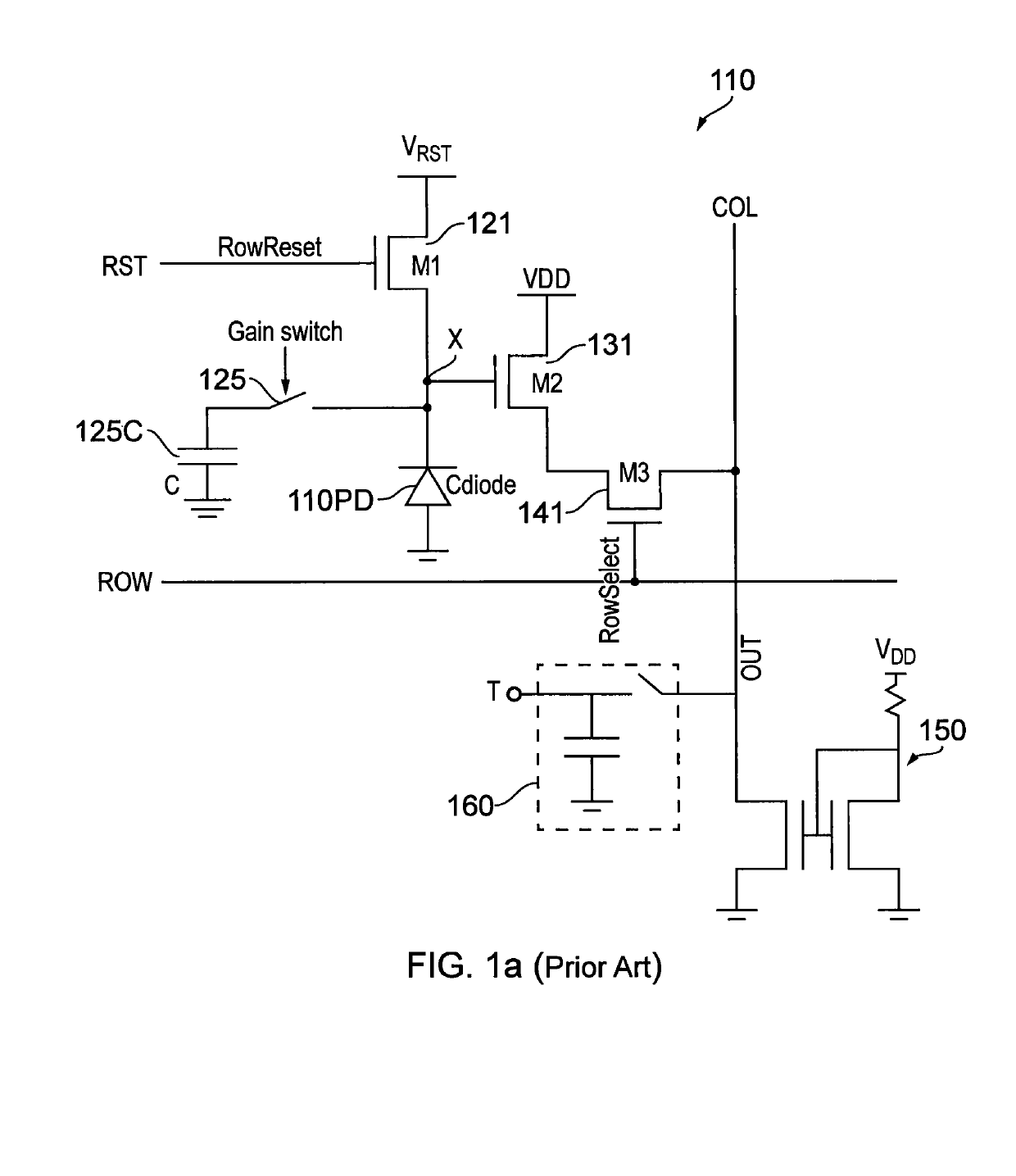
However, increasing the node capacitance causes an increase in the sampling noise (reset noise on node X) in the output signal of the pixel element 110 (i.e. the total potential read out at column line COL), reducing the signal to noise ratio (SNR) for relatively small signal levels.

Method used


Image

  • Radiation detection devices and methods
  • Radiation detection devices and methods
  • Radiation detection devices and methods

Examples


Embodiment Construction

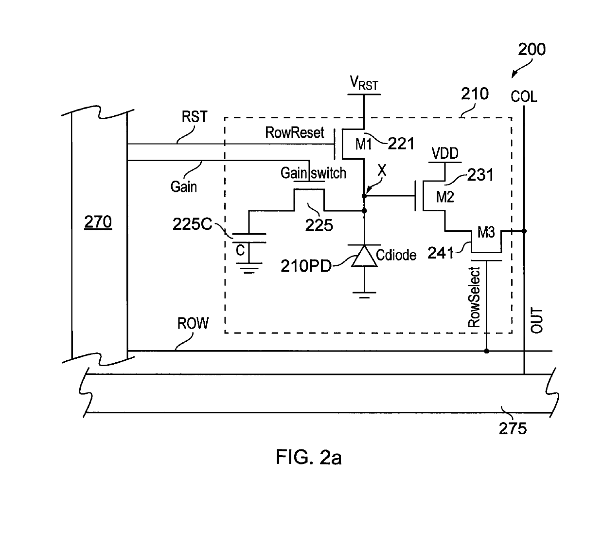
[0102]FIG. 2(a) is a schematic circuit diagram of a portion of a detector device 200 according to an embodiment of the present invention. The detector device 200 includes a pixel element 210. FIG. 2(b) is a further schematic illustration of the detector device 200. FIG. 2(c) is timing diagram associated with operation of the detector device 200.

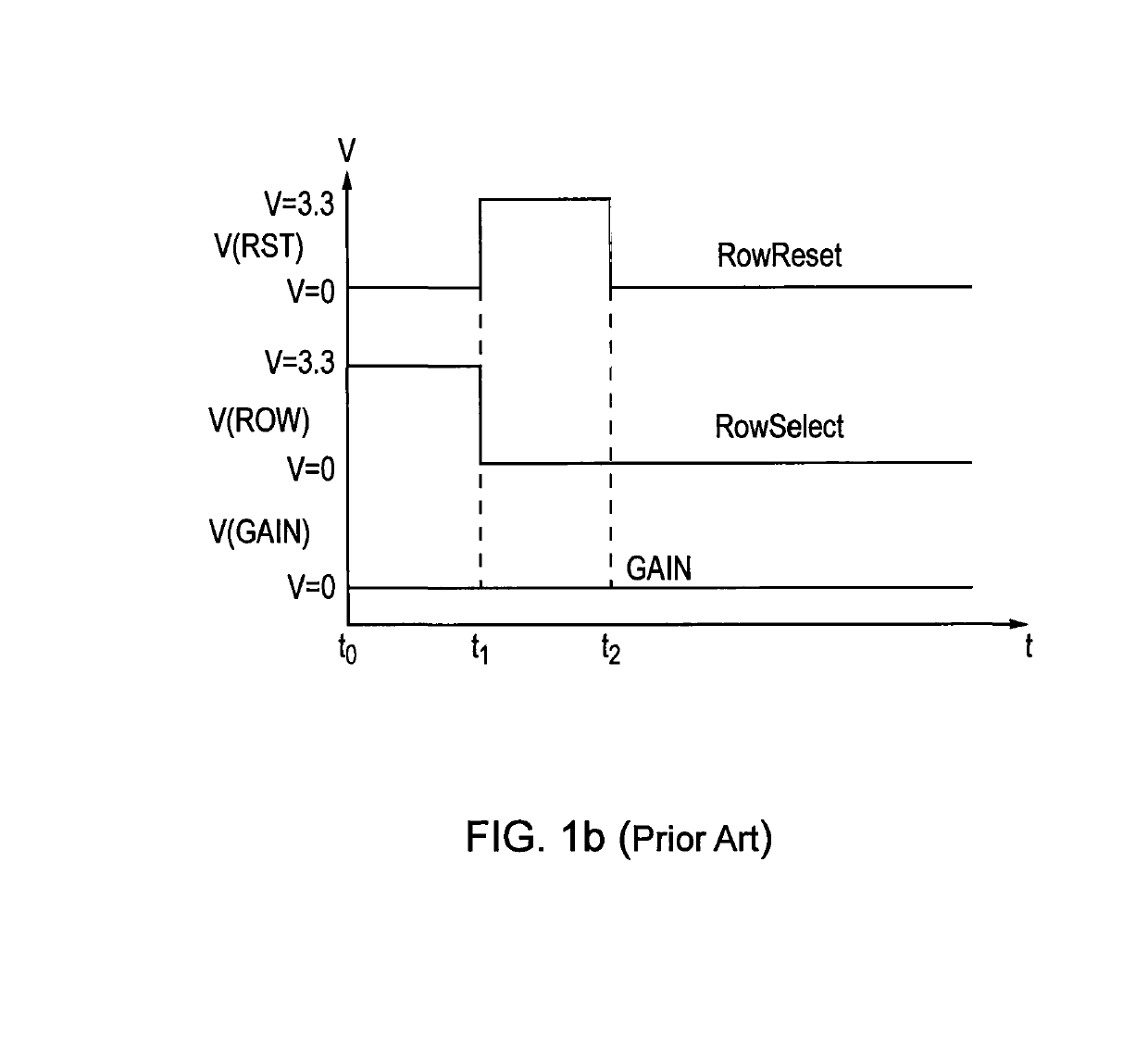
[0103]In FIG. 2(a), like features of the pixel element 210 to those of the element 110 of FIG. 1 are shown with like reference signs prefixed numeral 2 instead of numeral 1.

[0104]As can be seen from FIG. 2(a) the pixel element 210 has a gain control transistor device 225 coupled between the photodiode 210PD and capacitor device 225C. When gain control signal line GAIN is set high, the gain control transistor device 225 closes and the potential across the capacitor device 225C is set to the potential at node X.

[0105]The pixel element 210 may be operated in a low gain mode in which gain control transistor device 225 remains closed during the in...


PUM


Abstract

Embodiments of the present invention provide a detector comprising at least one detector element, the at least one detector element comprising: a photodiode element operable to generate charge carriers, the detector being configured to generate a signal indicative of a cumulative amount of charge carriers generated by the photodiode element during the integration period; a reset switch element configured to couple the photodiode element to a reset potential; at least one charge storage reservoir; and at least one gain control switch element configured to couple at least one said at least one charge storage reservoir to the photodiode element, wherein the detector is configured to perform a reset operation in which the reset switch element and at least one said at least one gain control switch element are closed in order to couple at least one said at least one charge storage reservoir and the photodiode element to the reset potential, the detector being configured to open at least one gain control switch element following a reset operation in dependence on whether at least one charge storage reservoir is to remain connected to the photodiode element during the integration period.

Description

RELATED APPLICATIONS[0001]This application is a 35 U.S.C. § 371 national stage application of PCT Application No. PCT / GB2015 / 051245, filed on Apr. 29, 2015, which claims priority from Great Britain Patent Application No. 1407552.7, filed Apr. 29, 2014, the contents of which are incorporated herein by reference in their entireties. The above-referenced PCT International Application was published in the English language as International Publication No. WO 2015 / 166238 A1 on Nov. 5, 2015.TECHNICAL FIELD[0002]The present invention relates to radiation detectors. In particular but not exclusively the invention relates to radiation detectors fabricated in silicon by means of CMOS wafer processing technologies.BACKGROUND[0003]It is known to provide an imaging device having a radiation detector in the form of a two dimensional array of pixels or pixel elements, each pixel element having a radiation sensor element for detecting radiation incident thereon. An image of a subject may be obtained...

Claims


Application Information

Patent Timeline
Patent Type & Authority Patents(United States)
IPC IPC(8): H04N3/14H04N5/3745H04N5/335H04N5/355H04N5/378H01L27/146H04N5/32
CPCH04N5/3559H01L27/14607H04N5/378H04N5/37452H01L27/14609H04N5/32H04N25/59H04N25/771H04N25/57H04N25/75
Inventor ANAXAGORAS, THALIS
Owner ISDI
Learn More