Metal of ceramic material hardened pattern

a technology of ceramic materials and hardened patterns, applied in the field of patterned structures, can solve the problems of not meeting the dsa patterned block copolymer lines

Active Publication Date: 2019-05-28
INTERUNIVERSITAIR MICRO ELECTRONICS CENT (IMEC VZW) +1
View PDF6 Cites 0 Cited by
  • Summary
  • Abstract
  • Description
  • Claims
  • Application Information

AI Technical Summary

Benefits of technology

[0006]It is an object of the present disclosure to provide good structures and methods for hardening the pattern of a first material while minimizing the alterations to the pattern or to the transfer thereof.
[0007]It is an advantage of embodiments of the present disclosure that toppling, such as bending or collapsing, or pitch walking of features of the pattern can be eliminated, or at least reduced.
[0008]It is an advantage of embodiments of the present disclosure that the pattern may be constructed using a self-assembled material.
[0009]It is an advantage of embodiments of the present disclosure that the patternmay be (anti-)aligned to guiding features in the underlying layer.
[0010]It is an advantage of embodiments of the present disclosure that the obtained pattern can be suitable as an etch mask to pattern the underlying substrate.

Problems solved by technology

However, it was reported that the DSA patterned block copolymer lines do not yet meet the semiconductor industry specification for the line edge roughness, i.e. a measure for the deviation between the actual shape of a pattern feature sidewall and its intended shape (typically quantified as 3 times the standard deviation from the intended shape), and line width roughness, i.e. a measure for the deviation between the actual width of a pattern feature and its intended width (typically quantified as 3 times the standard deviation of the width).

Method used


Image

  • Metal of ceramic material hardened pattern
  • Metal of ceramic material hardened pattern
  • Metal of ceramic material hardened pattern

Examples


example 1

Fabricating and Using a Patterned Structure According to the Present Disclosure

[0117]A patterned structure according to an embodiment of the present disclosure was made and used in patterning the substrate (100).

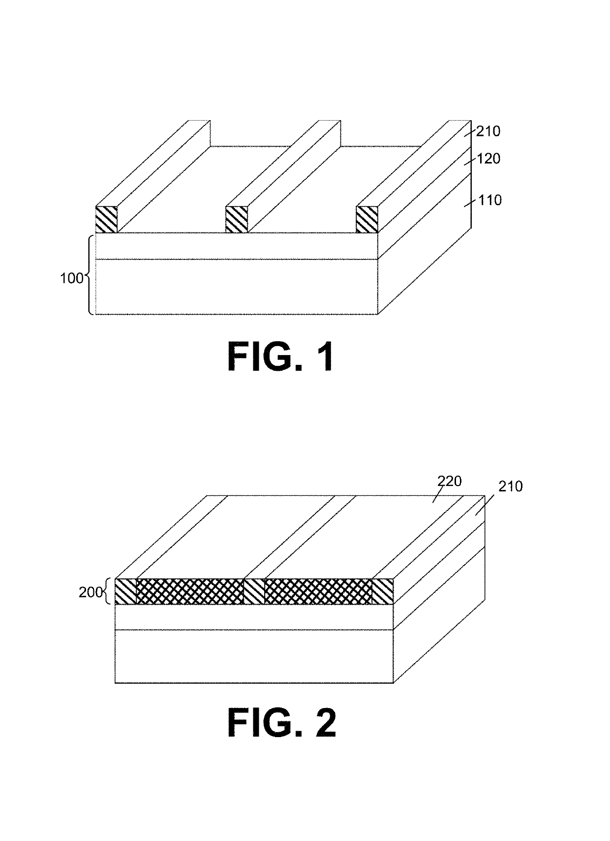
[0118]We now refer to FIG. 1. A substrate (100) was provided, comprising a Si wafer (110) and a spin-on-glass (SOG) hardmask (120) thereon. Lines of cross linkable PMMA (X-PMMA) guiding material (210) were lithographically fabricated onto this hardmask (120).

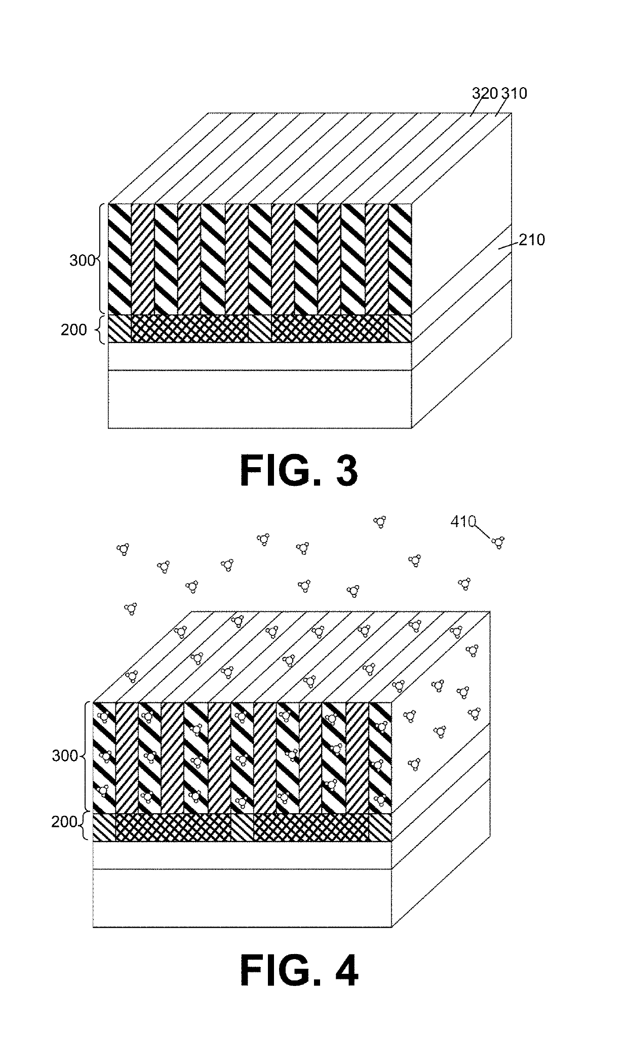
[0119]We now refer to FIG. 2. The gaps between the lines of X-PMMA guiding material (210) were filled with a PS-r-PMMA filler material (220) and subsequently annealed, completing the first layer (200). The thickness of the PS-r-PMMA filler material (220) was largely determined by its molecular weight, which was tuned to match the thickness of the X-PMMA guiding material (210), thus obtaining a first layer (200) with a planar surface.

[0120]We now refer to FIG. 3. A PS-b-PMMA block copolymer second layer (300) was self-ass...

example 2

Comparison Between the Hardened Pattern of the Conventional Method and the Present Disclosure

[0126]The steps in making the patterned structure according to embodiments of the present disclosure (part b of FIGS. 9 to 12) will be compared to a conventional method (part a of FIGS. 9 to 12).

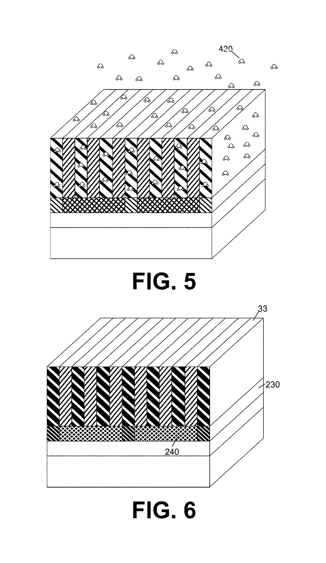
[0127]We now refer to FIG. 9. We start from a structure comprising a substrate (100) with a hardmask layer (120), a first layer (200) with zones of guiding material (250, 210) in a matrix of filler material (220) and a second layer (300) comprising a pattern of a first material (310) in a matrix of a further material (320). The second layer (300) may for example comprise a self-assembled PS-b-PMMA block copolymer, comprising sections of PMMA first material (310) and sections of PS further material (320). The structure of the present disclosure differs at this point from a structure prepared by a convention method in the nature of the guiding material (250, 210): in conventional methods (FIG. 9, part ...


PUM

PropertyMeasurementUnit
volume fractionaaaaaaaaaa
wetting affinityaaaaaaaaaa
edge roughnessaaaaaaaaaa

Abstract

The present disclosure relates to a patterned structure, the structure comprising:i) a substrate,ii) a first layer on top of the substrate, comprising a filler material and a guiding material, wherein at least a top surface of the first layer comprises one or more zones of filler material and one or more zones of guiding material, andiii) a second layer on top of the first layer comprising a pattern of a first material, the pattern being either aligned or anti-aligned with the underlying one or more zones of guiding material;wherein the first material comprises a metal or a ceramic material and wherein the guiding material and the filler material either both comprise or both do not comprise the metal or ceramic material.

Description

RELATED APPLICATION[0001]This application claims priority from EP 16156539.5, filed Feb. 19, 2016, which is incorporated by reference in its entirety.TECHNICAL FIELD OF THE DISCLOSURE[0002]The present disclosure relates to patterned structures for use in the semiconductor industry, and in particular to such patterned structures where the pattern is hardened with a metal or ceramic material.BACKGROUND OF THE DISCLOSURE[0003]Patterned materials, such as obtained through the directed self-assembly (DSA) of block copolymers, has been proposed for making etch masks. DSA of block copolymers uses guiding features in a sublayer to direct the block copolymer film formation. After the block copolymer components self-assemble on the sublayer, one of the polymer blocks can be selectively removed, leaving the other block with the desired pattern. This patterned block can in turn be used as an etch mask to transfer the pattern into an underlying substrate (100); for example for use in semiconduct...

Claims


Application Information

Patent Timeline
Patent Type & Authority Patents(United States)
IPC IPC(8): B32B7/00G03F7/00H01L21/027H01L21/033
CPCG03F7/0002H01L21/0271H01L21/0337Y10T428/24926Y10T428/24917H01L21/027H01L23/13
Inventor CHAN, BOON TEIKSINGH, ARJUNSAYAN, SAFAK
Owner INTERUNIVERSITAIR MICRO ELECTRONICS CENT (IMEC VZW)
Why Eureka
Try Eureka