Scan driver circuit and liquid crystal display device having the circuit

a driving circuit and liquid crystal display technology, applied in the field of display technology, can solve problems affecting the quality of the display of images, and achieve the effects of improving the uniformity of the common-mode signal voltage, effective reduction of sensing voltage, and improving display quality

Active Publication Date: 2019-10-29
WUHAN CHINA STAR OPTOELECTRONICS TECH CO LTD
View PDF7 Cites 1 Cited by
  • Summary
  • Abstract
  • Description
  • Claims
  • Application Information

AI Technical Summary

Benefits of technology

[0003]The present application to solve the technical problem is to provide a scanning driving circuit and a flat display apparatus having the scanning driving circuit to effectively decreasing the sensing voltage, and further improving the uniformity of the common-mode signal voltage in the panel and improve the quality of the display of the image.
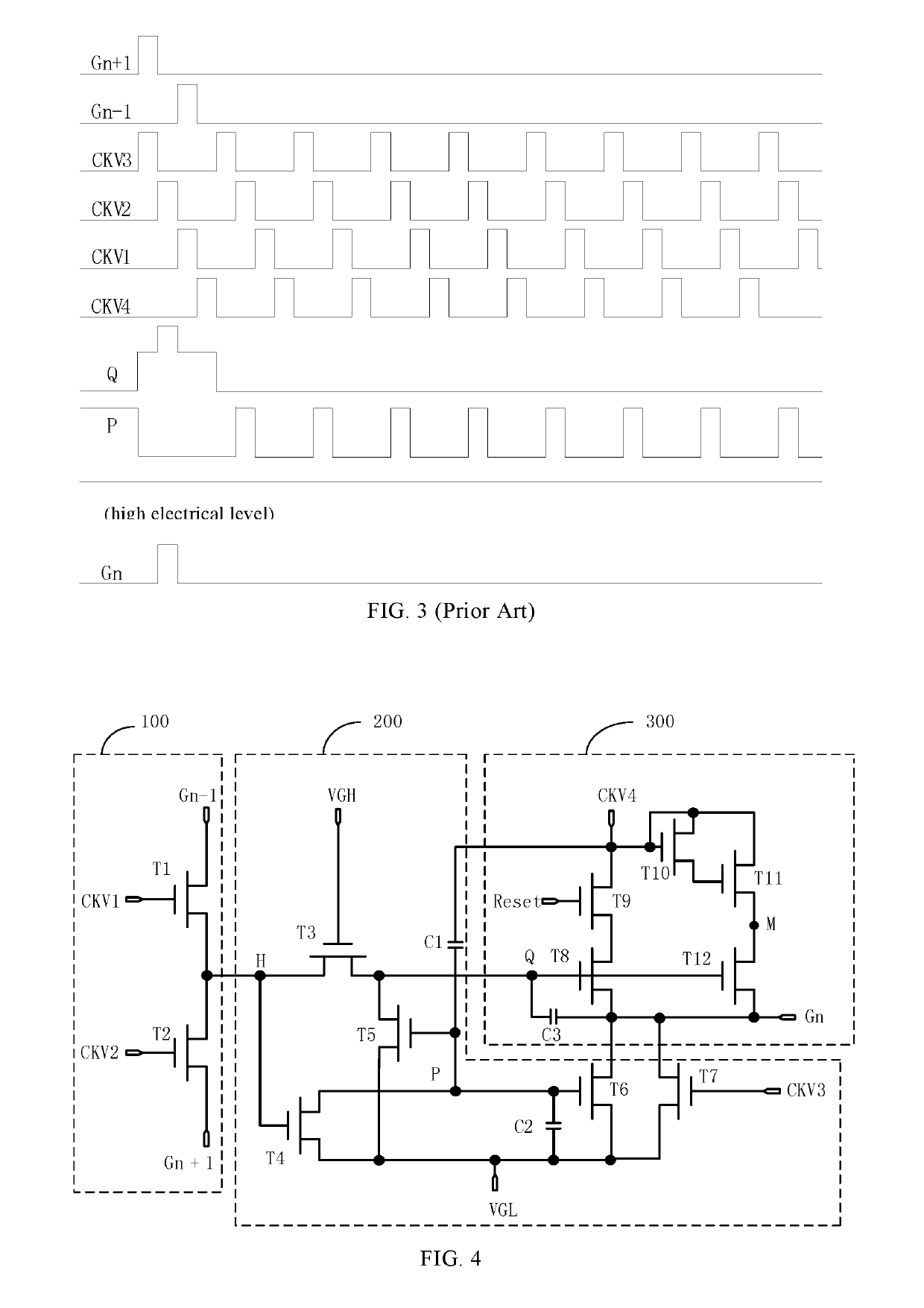
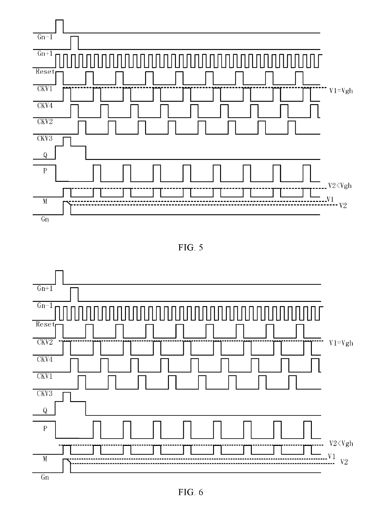
[0031]The advantage of the present application is, comparing to the conventional technology, the scanning driving circuit of the present application performs the forward scanning and reverse scanning by the scanning driving circuit controlled by the forward and reverse scanning circuit, and by the input circuit to charge the pull-up control signal point and the pull-down control signal point, by the output circuit to generate the scanning driving signal with two-valued high electrical level output to the scanning line to drive the pixel unit to thereby effectively decreasing the sensing voltage, and further improving the uniformity of the common-mode signal voltage in the panel and improve the quality of the display of the image.

Problems solved by technology

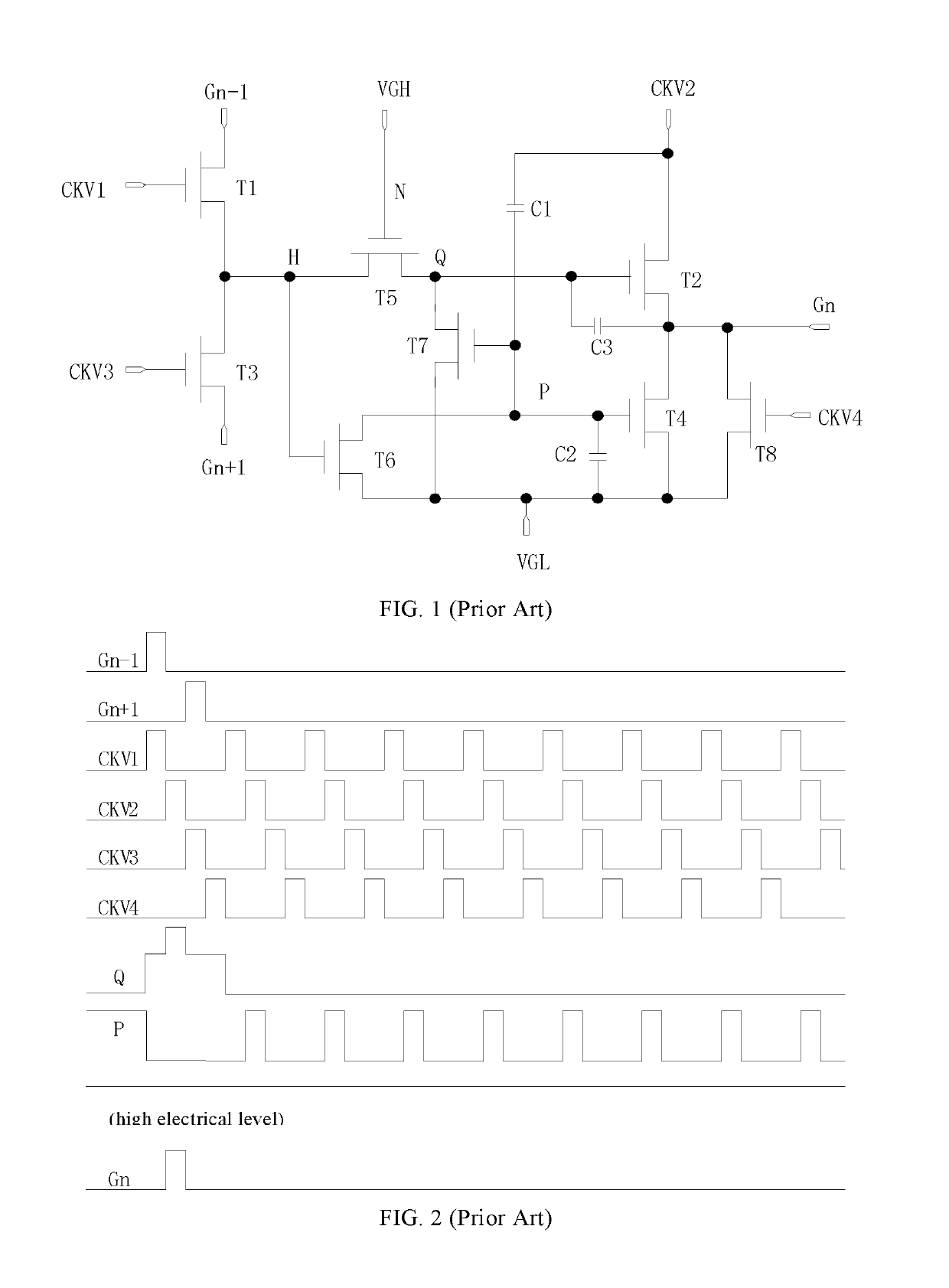
The corresponding sensing voltage of this driving mode is large, which causes the optimization common-mode signal voltage corresponding to different area of the panel is inconsistent, that is the two-valued driving is likely to cause the poor uniformity of the common-mode signal voltage of the panel, affecting the quality of the display of the image.

Method used


Image

  • Scan driver circuit and liquid crystal display device having the circuit
  • Scan driver circuit and liquid crystal display device having the circuit
  • Scan driver circuit and liquid crystal display device having the circuit

Examples


Embodiment Construction

[0041]Embodiments of the present application are described in detail with the technical matters, structural features, achieved objects, and effects with reference to the accompanying drawings as follows. It is clear that the described embodiments are part of embodiments of the present application, but not all embodiments. Based on the embodiments of the present application, all other embodiments to those of ordinary skill in the premise of no creative efforts obtained should be considered within the scope of protection of the present application.

[0042]Specifically, the terminologies in the embodiments of the present application are merely for describing the purpose of the certain embodiment, but not to limit the invention. Examples and the claims be implemented in the present application requires the use of the singular form of the book “an”, “the” and “the” are intend to include most forms unless the context clearly dictates otherwise. It should also be understood that the terminol...


PUM


Abstract

The present application discloses a scanning driving circuit and a flat display apparatus, the scanning driving circuit includes a plurality of cascaded scanning driving unit, each scanning driving unit including a forward and reverse scanning circuit for controlling the forward or reverse scanning; an input circuit to perform charging to the pull-up control signal point and the pull-down control signal point; an output circuit for generating a scanning driving signal with two-valued high electrical level and outputting to the current level scanning line to drive a pixel unit.

Description

FIELD OF THE INVENTION[0001]The present application relates to a display technology field, and more particularly to a scanning driving circuit and a flat display apparatus having the scanning driving circuit.BACKGROUND OF THE INVENTION[0002]A scanning driving circuit is used in the flat panel display device currently, which is forming the scanning driving circuit on the array substrate by using the conventional thin-film transistor array process of the flat panel display, to achieve the driving mode of scanning row by row. The output high and low electrical level of the current level of the scanning line of the scanning driving circuit in the conventional technology is the turn-on voltage terminal signal and the turn-off voltage terminal signal, respectively, and is two-valued driving. The corresponding sensing voltage of this driving mode is large, which causes the optimization common-mode signal voltage corresponding to different area of the panel is inconsistent, that is the two-...

Claims


Application Information

Patent Timeline
Patent Type & Authority Patents(United States)
IPC IPC(8): G09G3/3208G09G3/36
CPCG09G3/3208G09G3/36G09G3/3648G09G2310/08G09G2310/0267G09G3/3266G09G3/3677G09G2310/0286G09G2310/0213
Inventor LI, YAFENG
Owner WUHAN CHINA STAR OPTOELECTRONICS TECH CO LTD
Why Eureka
Try Eureka