Solid-state imaging device with on chip lenses with adjust characteristics to render pixel output sensitivities more uniform

Inactive Publication Date: 2013-06-04
SONY SEMICON SOLUTIONS CORP
View PDF15 Cites 0 Cited by
  • Summary
  • Abstract
  • Description
  • Claims
  • Application Information

AI Technical Summary

Benefits of technology

[0019]In the solid-state imaging device and the camera according to embodiments of the present invention, the deterioration of the image quality periodically

Problems solved by technology

Therefore, because the light sensing units and interconnection layers are not disposed regularly, or in other words, because patterns formed for the light sensing units and the interconnection layers are non-uniform p

Method used


Image

  • Solid-state imaging device with on chip lenses with adjust characteristics to render pixel output sensitivities more uniform
  • Solid-state imaging device with on chip lenses with adjust characteristics to render pixel output sensitivities more uniform
  • Solid-state imaging device with on chip lenses with adjust characteristics to render pixel output sensitivities more uniform

Examples


first embodiment

1. First Embodiment

[Schematic Configuration of Solid-State Imaging Device]

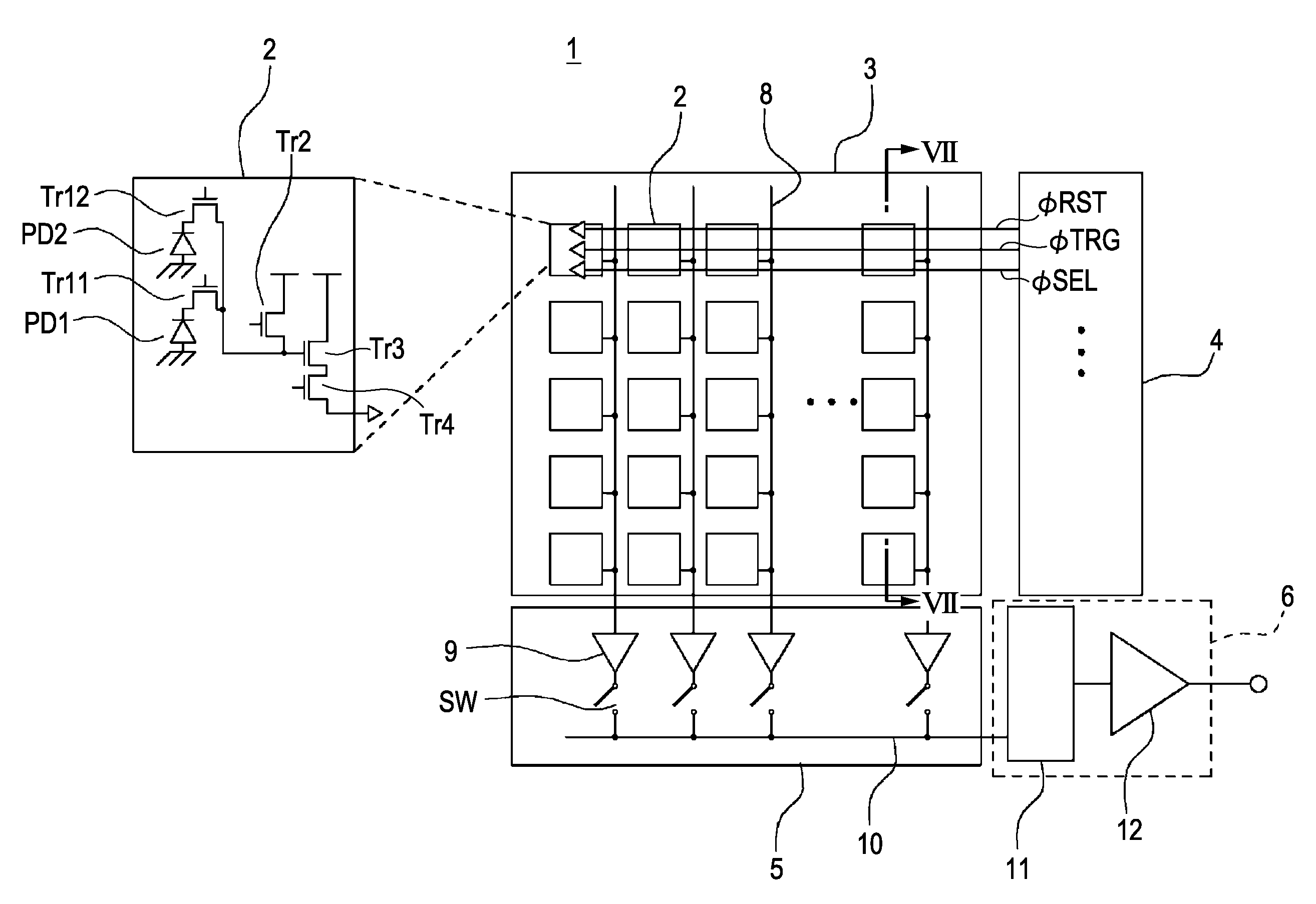
[0047]FIG. 1 is a schematic configuration diagram of a CMOS-type image sensor that is an example of a solid-state imaging device according to an embodiment of the present invention. In the CMOS-type image sensor shown in FIG. 1, plural sets of two pixels sharing a reset transistor Tr2, an amplifying transistor Tr3, and a selection transistor Tr4 are arranged in a matrix. A set of two pixels sharing a reset transistor Tr2, an amplifying transistor Tr3, and a selection transistor Tr4 will be referred to as a component-shared-by-two-pixels unit hereinafter.

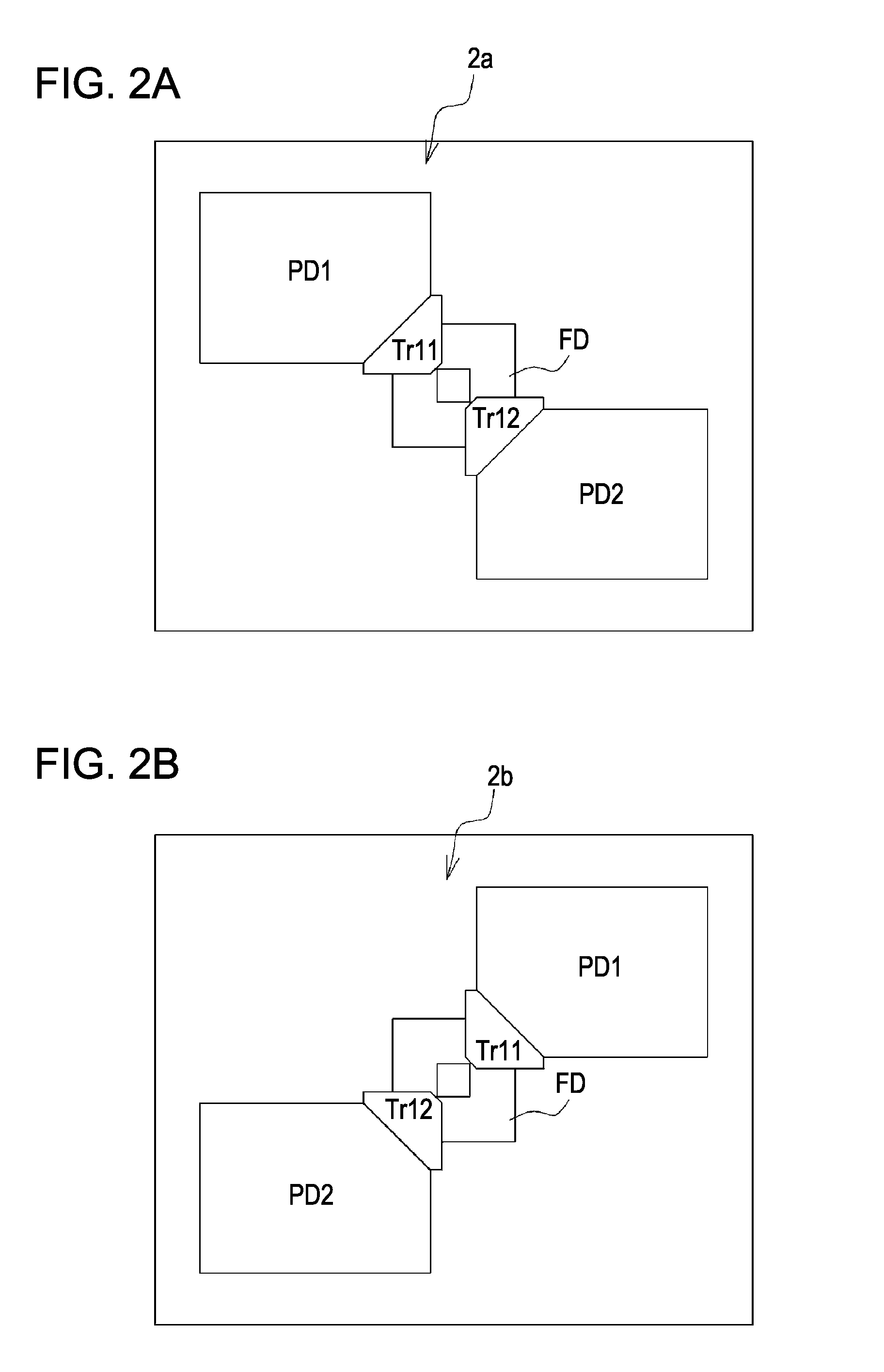
[0048]To put it more precisely, two photodiodes PD1 and PD2, and two transfer transistors Tr11 and Tr12, which correspond to the photodiodes PD1 and PD2 respectively, share the reset transistor Tr2, the amplifying transistor Tr3, and the selection transistor Tr4.

[0049]FIG. 1 shows that the CMOS-type image sensor 1 according to a first embodiment is composed of ...

second embodiment

2. A Second Embodiment

[A Configuration of a Camera]

[0113]FIG. 12 is a schematic configuration diagram of an example of a CMOS-type camera according to another embodiment of the present invention is employed. The above-described CMOS-type image sensor according to the first embodiment is employed as an imaging device in this camera 77.

[0114]The camera 77 according to this embodiment of the present invention is configured so that incident lights from an object (not shown in FIG. 12) enter an imaging unit of a solid-state imaging device 73 through an optical system such as a lens 71 and a mechanical shutter 72. The mechanical shutter 72 is used for setting the exposure time by conducting or shutting out the incident lights to / from the imaging unit of the solid-state imaging device 73.

[0115]In this camera, the above-described solid-state imaging device according to the first embodiment is used as the solid-state imaging device 73, and this solid-state imaging device 73 is driven by a dr...


PUM


Abstract

A solid-state imaging device includes: an imaging unit wherein a plurality of light sensing units formed in a matrix and a plurality of interconnections are formed among the plurality of light sensing units; a color filter that is disposed over the imaging unit, and delivers colors to the light sensing units in accordance with a predefined rule; and on-chip lenses that are disposed corresponding to the light sensing units on a one-by-one basis over the color filter, and have light-collection characteristics varying in accordance with differences among sensitivities of the light sensing units, where the differences among the sensitivities of the light sensing units are generated, when the same colors are delivered to the light sensing units in accordance with the same rule, owing to the fact that positions of the individual interconnections relative to the light sensing units vary periodically.

Description

BACKGROUND OF THE INVENTION[0001]1. Field of the Invention[0002]The present invention relates to solid-state imaging devices, and cameras, and more particularly relates to a solid-state imaging device in which positional relations between light sensing units and interconnection layers vary periodically, and a camera equipped with such a solid-state imaging device.[0003]2. Description of the Related Art[0004]In recent years, a CMOS-type solid-state imaging device, to which CMOS (complementary metal oxide semiconductor) technology, which is one of standard technologies for IC manufacturing is applied, has been in widespread use.[0005]Being different from a CCD (charge coupled device)-type solid-state imaging device, a CMOS-type solid-state imaging device does not use high driving voltages, and can be integrated (disposed on-chip) with peripheral circuits, which brings about a great advantage to miniaturization of the solid-state imaging device.[0006]In addition, miniaturization and mu...

Claims


Application Information

Patent Timeline
IPC IPC(8): H04N9/07H04N5/335H04N9/04
CPCH04N5/3696H04N9/045H04N5/37457H01L27/14612H01L27/14621H01L27/14627H01L27/14645H04N25/778H04N25/134
Inventor HAMADA, KAZUHIKO
Owner SONY SEMICON SOLUTIONS CORP
Why Eureka
Try Eureka