The embodiments of the present disclosure provide a liquid crystal display device and a method for manufacturing the same, so as to at least partially eliminate or alleviate one or more of the plurality of technical problems as mentioned above.
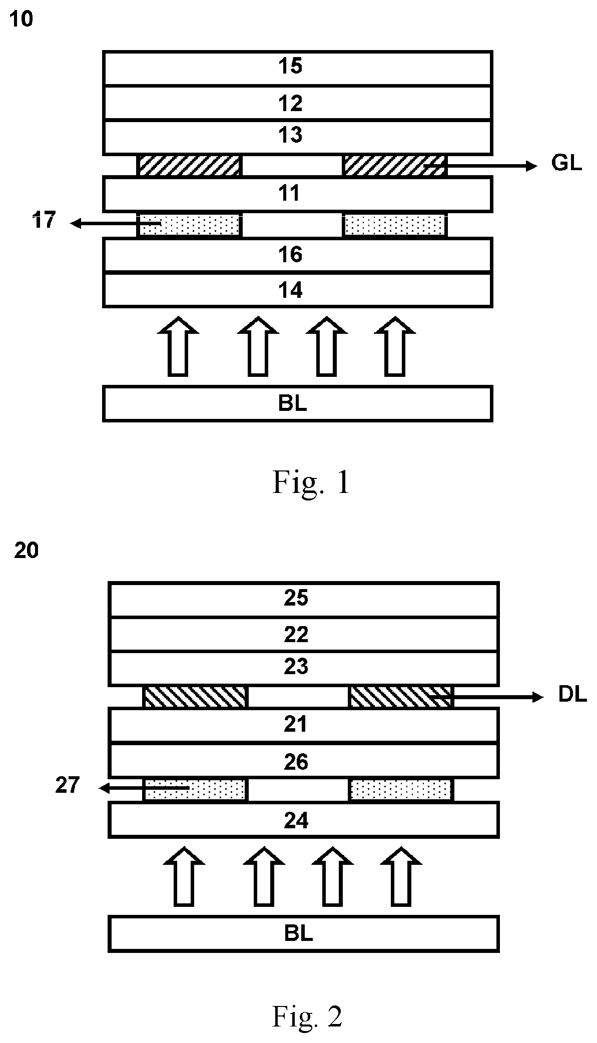
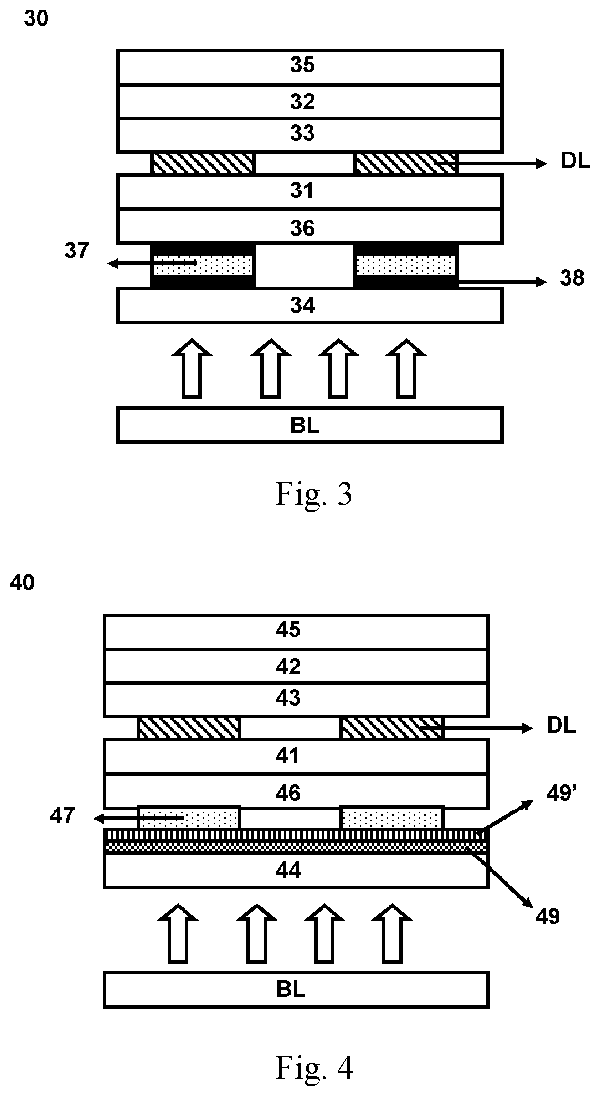
In the liquid crystal display device according to this aspect of the present disclosure, the reflective grid is formed on the light incident side of the liquid crystal display panel, namely between the array substrate and the light guide plate. Besides, such a reflective grid corresponds to the gate line or data line on the array substrate in terms of shape and position, in such a way that the backlight that could otherwise have been incident on the gate line or data line of the array substrate will be reflected by the reflective grid provided according to this aspect of the present disclosure, and then can return to the display panel through further reflection by the light guide plate. Thus, the display device according to this aspect of the present disclosure not only enhances the utilization rate of backlight, but also reduces the requirement for the aperture ratio of the display pixel. As an example, the material for making the reflective grid as mentioned above may comprise silver and the like, and may have a thickness of e.g. 100 nm. Of course, the present disclosure is not limited to such an exemplary material, and those skilled in the art can readily obtain the appropriate material composition for the reflective grid and further the thickness setting according to specific practical demands.
According to a specific embodiment, in the liquid crystal display device as mentioned above, the light guide plate further comprises a reflective film disposed on the side of the light guide plate facing the array substrate. Alternatively, according to another specific embodiment, the light guide plate further comprises an optical compensation film on the side of the light guide plate facing the array substrate. The reflective film additionally provided for the light guide plate facilitates further reflection of the light reflected by the reflective grid, which is helpful for the improvement on repeated utilization of backlight. Moreover, different types of optical compensation films, such as phase compensation or color difference compensation, can greatly improve the quality of backlight emission and therefore guarantee excellent display performance of the liquid crystal display device.
Similar to the depiction of the liquid crystal display device according to the first aspect, in the method for manufacturing a liquid crystal display device according to this aspect of the present disclosure, the backlight that could otherwise have been incident on the gate line or data line can be reflected by the reflective grid that is separately formed, and be further reflected additionally by the light guide plate back to the liquid crystal panel. Thus, it not only enhances the utilization rate of backlight, but also reduces the requirement for the aperture ratio of the display pixel.
According to a specific embodiment, the method for manufacturing a liquid crystal display device as mentioned above further comprises: forming a protective layer on the side of the second polarizer facing the light guide plate before forming the reflective layer. Alternatively, in another specific embodiment, the method for manufacturing a liquid crystal display device as mentioned above further comprises: forming a protective layer covering the reflective grid after forming the reflective grid. With reference to the specific depiction about the liquid crystal display device, the provision of such a protective layer is helpful for enhanced protection of the reflective grid, which further ensures the operational performance and corresponding display quality of the liquid crystal display device.
According to another specific embodiment, in the method for manufacturing a liquid crystal display device as mentioned above, the step of forming a reflective grid comprises: forming a reflective grid on a side of a transparent layer; and attaching the transparent layer having the reflective grid entirely to the side of the second polarizer facing the light guide plate by means of a high-precision aligned attachment technique. In such an implementation, the reflective grid is first formed on another transparent layer (namely, another medium) and then entirely attached to the second polarizer. According to such a manufacturing process, attachment of the reflective grid to the second polarizer by means of another auxiliary medium reduces the operational difficulty and facilitates improvement in processing speed.

