
Organic light emitting diode screen and manufacturing method thereof

a technology of light-emitting diodes and organic glass, which is applied in the direction of basic electric elements, electrical equipment, semiconductor devices, etc., can solve the problems of low yield rate of 3d glass, high cost, and inability to achieve frameless effect, so as to improve the frameless display effect and enhance the mirror effect

Active Publication Date: 2020-05-26
WUHAN CHINA STAR OPTOELECTRONICS SEMICON DISPLAY TECH CO LTD
View PDF5 Cites 1 Cited by
  • Summary
  • Abstract
  • Description
  • Claims
  • Application Information

AI Technical Summary

Benefits of technology

[0004]An objective of the present invention is to provide an organic light emitting diode screen and a manufacturing method thereof, which can achieve a frameless display effect.
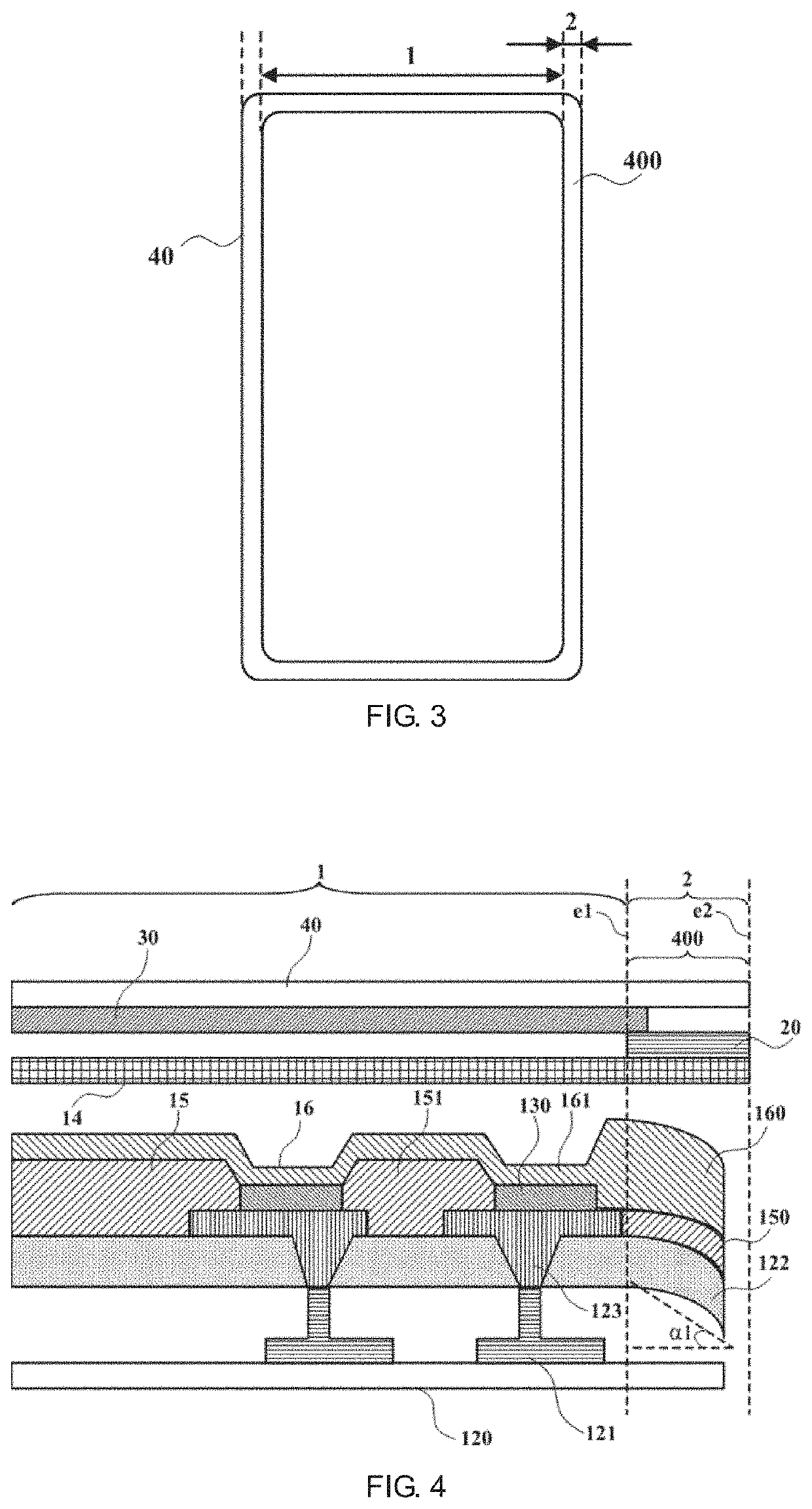
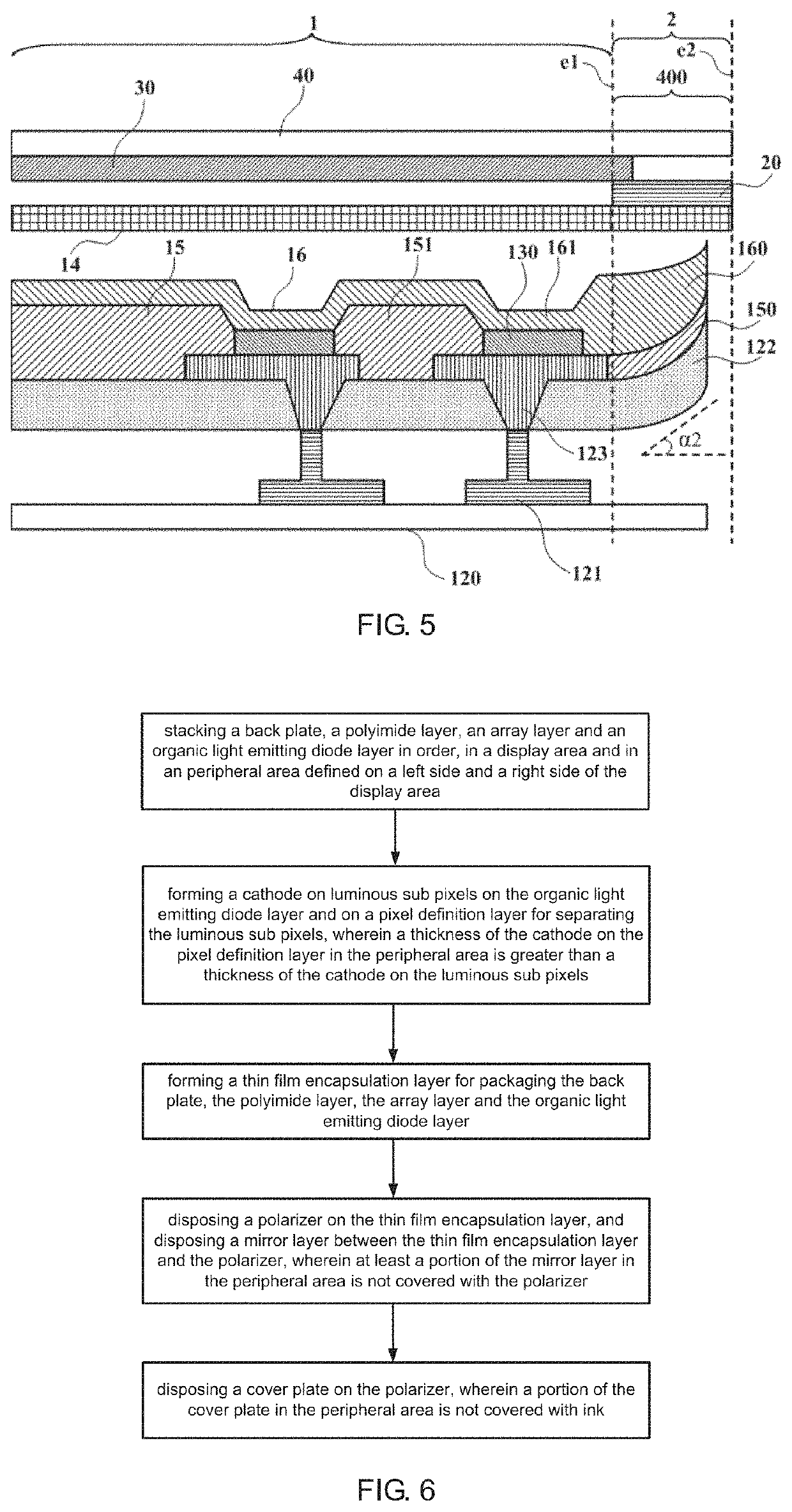
[0024]The benefits of the embodiment of the present invention are: a mirror layer is disposed in the peripheral area on the left side and the right side of the display area, at least a portion of the mirror layer is not covered by the polarizer thereon, and the cover plate on the polarizer is also not covered with ink. When the organic light emitting diode screen is lit, the light emitted by the organic light emitting diode layer can be transmitted out of the peripheral area to achieve a frameless display effect; when the organic light emitting diode layer does not emit light, the mirror layer can reflect the external light to achieve the display effect of the mirror-type organic light emitting diode screen, and can prevent the traces in the peripheral area from being observed from the outside;
[0025]the cathode on the pixel definition layer in the peripheral area is thickened, such that a thickness of the cathode on the pixel definition layer is greater than a thickness of the cathode on the luminous sub pixels for further enhancing the mirror effect;
[0026]the cathode, the pixel definition layer and the planarization layer in the peripheral area are bent for facilitating the light emitted by the luminous sub pixels near the peripheral area to be reflected at an appropriate angle to form a better frameless display effect.

Problems solved by technology

However, the 3D glass has a low yield rate and a high cost.
The frameless effect cannot be achieved.

Method used


Image

  • Organic light emitting diode screen and manufacturing method thereof
  • Organic light emitting diode screen and manufacturing method thereof
  • Organic light emitting diode screen and manufacturing method thereof

Examples


Embodiment Construction

[0034]The following descriptions for the respective embodiments are specific embodiments capable of being implemented for illustrations of the present invention with referring to appended figures.

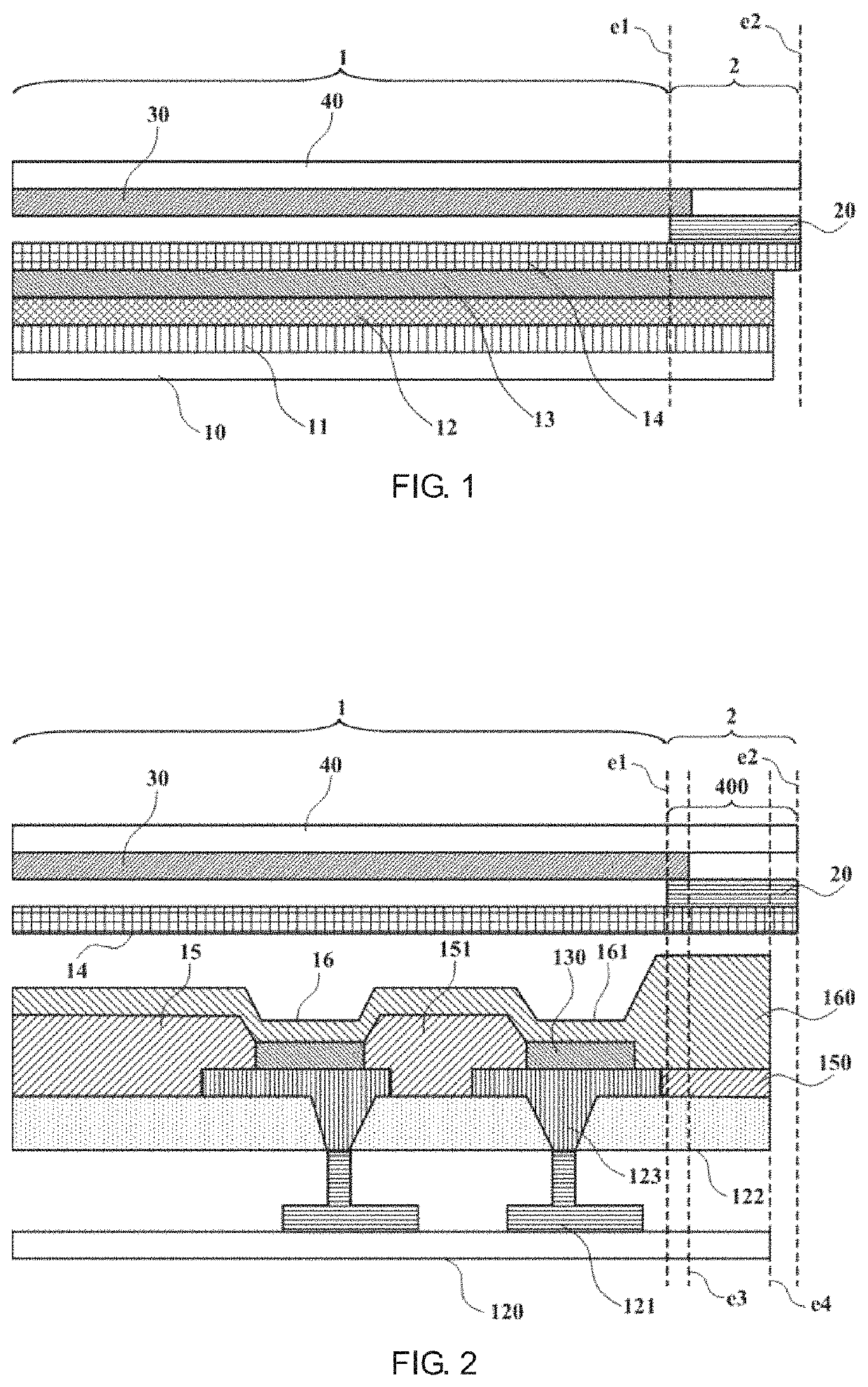
[0035]Please refer to FIG. 1. The first embodiment of the present invention provides an organic light emitting diode screen, having a display area 1 and a peripheral area 2 located on a left side and a right side of the display area 1, wherein the organic light emitting diode screen comprises:

[0036]a back plate 10, a polyimide layer 11, an array layer 12, an organic light emitting diode layer 13, a thin film encapsulation layer 14, a polarizer 30 and a cover plate 40 stacked in order;

[0037]wherein a mirror layer 20 is disposed between the thin film encapsulation layer 14 and the polarizer 30, and at least a portion of the mirror layer 20 in the peripheral area 2 is not covered with the polarizer 30;

[0038]a portion 400 of the cover plate 40 in the peripheral area 2 is not covered with ink.

[0...


PUM

PropertyMeasurementUnit
bending angleaaaaaaaaaa
widthaaaaaaaaaa
bending angle α2aaaaaaaaaa

Abstract

Provided are an OLED screen and a manufacturing method thereof. The OLED screen has a display area and a peripheral area located on a left side and a right side of the display area. The OLED screen comprises: a back plate, a polyimide layer, an array layer, an OLED layer, a thin film encapsulation layer, a polarizer and a cover plate stacked in order; a mirror layer is disposed between the thin film encapsulation layer and the polarizer, and at least a portion of the mirror layer in the peripheral area is not covered with the polarizer; a portion of the cover plate in the peripheral area is not covered with ink. When the organic light emitting diode screen is lit, the light emitted by the organic light emitting diode layer can be transmitted out of the peripheral area to achieve a frameless display effect.

Description

CROSS-REFERENCE TO RELATED APPLICATION[0001]This application is a continuing application of PCT Patent Application No. PCT / CN2018 / 089412 entitled “Organic light emitting diode screen and manufacturing method thereof”, filed on May 31, 2018, which claims priority to Chinese Patent Application No. 201810372504.4, filed on Apr. 24, 2018, both of which are hereby incorporated in its entireties by reference.FIELD OF THE INVENTION[0002]The present invention relates to a screen display field, and more particularly to an organic light emitting diode screen and a manufacturing method thereof.BACKGROUND OF THE INVENTION[0003]At present, the ultra-narrow frame is pursued for the mobile phone market. Even being frameless may become the mainstream. Major mobile phone manufacturing companies and screen research, development and manufacturing companies are actively developing in research and development of related technologies. The organic light emitting diode screen can realize the effect of bend...

Claims


Application Information

Patent Timeline
Patent Type & Authority Patents(United States)
IPC IPC(8): H01L27/32H01L51/52H01L51/56
CPCH01L51/5293H01L51/5221H01L51/5253H01L51/56H01L27/3246H01L51/5271H01L27/3258H01L2227/323H10K59/122H10K59/12H10K50/82H10K50/86H10K50/844H10K2102/351H10K50/856H10K50/868H10K59/124H10K71/00H10K59/1201
Inventor CAO, HAORANCHUN, PILGEUN
Owner WUHAN CHINA STAR OPTOELECTRONICS SEMICON DISPLAY TECH CO LTD
Learn More