
TFT substrate

a thin film transistor and substrate technology, applied in the field of display technology, can solve the problems of color shifting at a large view angle, short charging time and insufficient charging rate of pixels, and affect the level of written pixel voltage, so as to avoid poor displaying

Active Publication Date: 2020-06-02
SHENZHEN CHINA STAR OPTOELECTRONICS SEMICON DISPLAY TECH CO LTD
View PDF9 Cites 0 Cited by
  • Summary
  • Abstract
  • Description
  • Claims
  • Application Information

AI Technical Summary

Benefits of technology

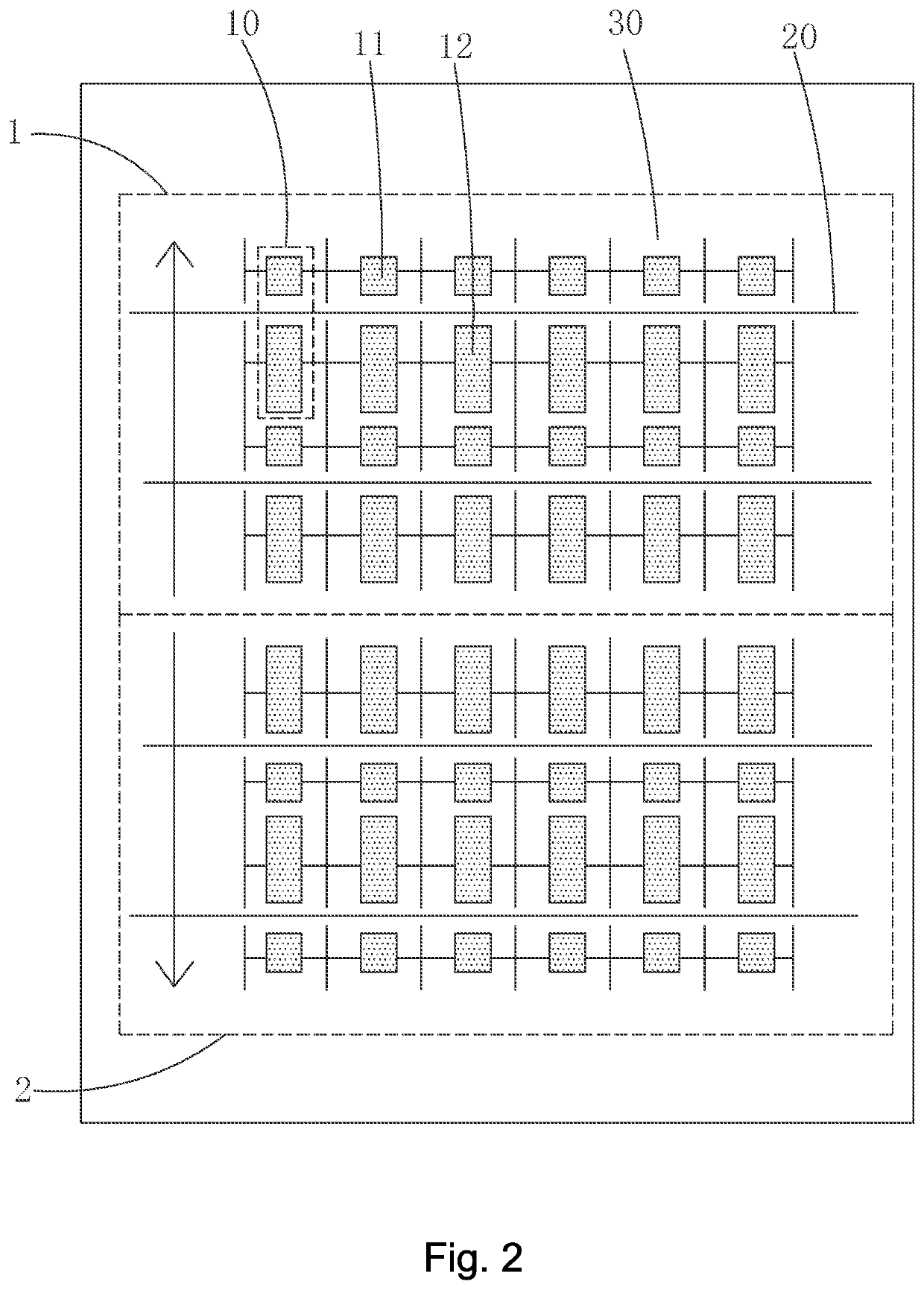
The present invention provides a thin-film transistor (TFT) substrate that prevents a coupling signal from affecting electrical voltage of a sub pixel electrode and ensures similar displaying effect for two display areas of a screen-split arrangement to thereby eliminate poor displaying. This is achieved by arranging main pixel electrodes and sub pixel electrodes in mirror symmetry with respect to each other. The scanning directions of the two display areas are such that both generate a coupling signal during scanning and write the pixel voltage to prevent the coupling signal from affecting the sub pixel electrode.

Problems solved by technology

One drawback of the large-sized screens is color shifting at a large view angle.
Potential risks caused by high resolution and high refresh rate are issues concerning short charging time and insufficient charging rate of pixels.
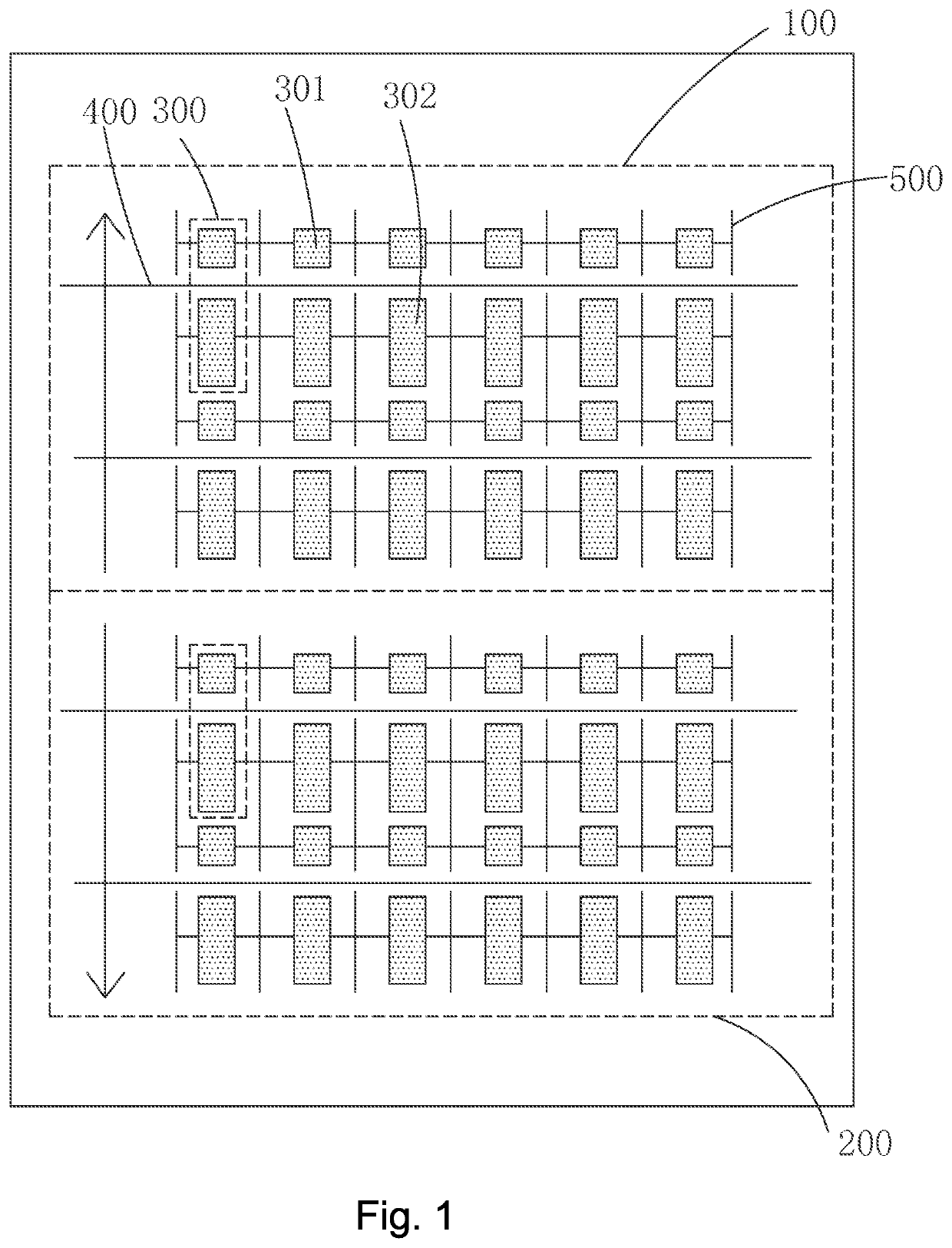
Particularly, in the lower display area 200, the coupling signal is generated in the sub pixel electrode 301 that have already been written with pixel voltages, and consequently, the levels of the written pixel voltages will be affected, leading to poor displaying.

Method used


Image

  • TFT substrate
  • TFT substrate
  • TFT substrate

Examples


Embodiment Construction

[0042]To further expound the technical solution adopted in the present invention and the advantages thereof, a detailed description will be given with reference to the preferred embodiments of the present invention and the drawings thereof.

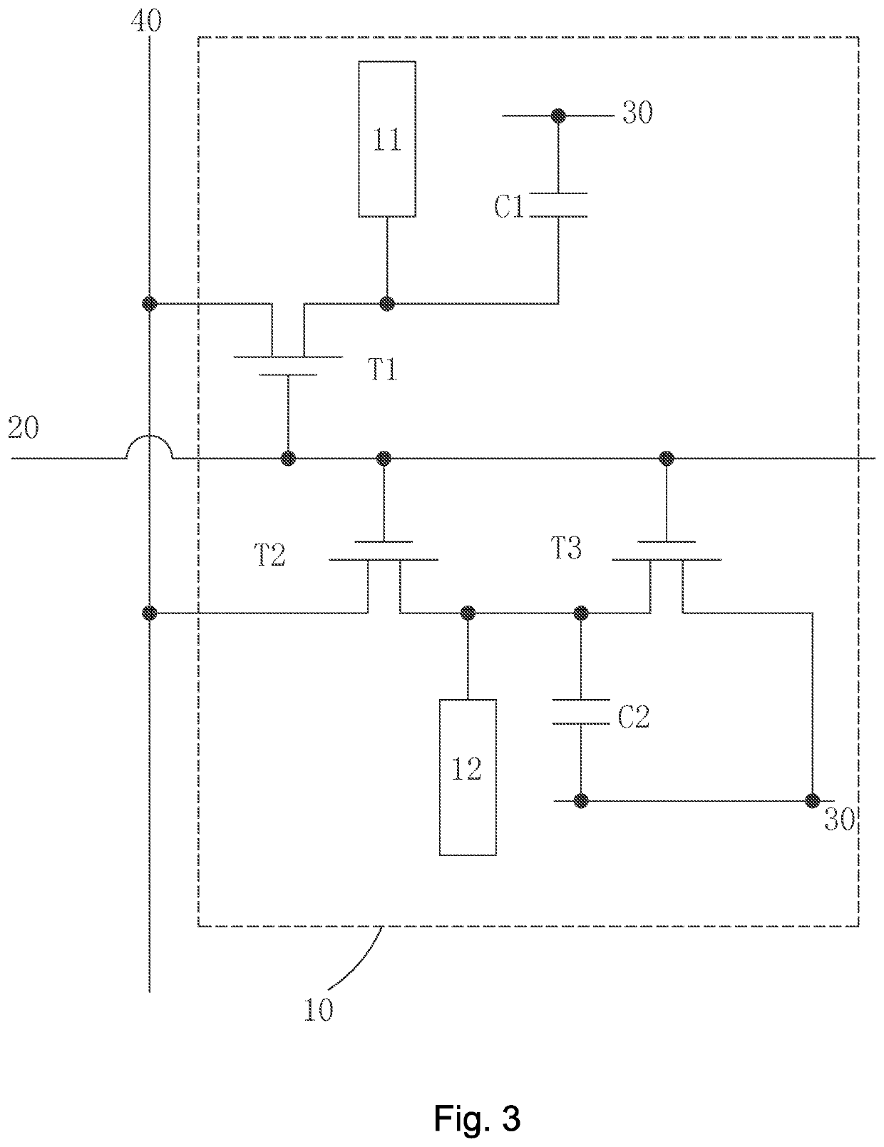
[0043]Referring to FIG. 2, as a first embodiment of the present invention, the present invention provides a thin-film transistor (TFT) substrate, which comprises: a first display area 1 and a second display area 2 that are arranged sequentially in a vertical direction. The first display area 1 and the second display area 2 each comprise: a plurality of sub-pixels 10 arranged in an array, a plurality of scan lines 20 that are arranged parallel to and spaced from each other and extend in a horizontal direction, and a plurality of array substrate common electrode lines 30. Each of rows of the sub-pixels 10 corresponds to one of the scan lines 20, and each of the sub-pixels 10 comprises: a main pixel electrode 11 and a sub pixel electrode 12 respectiv...


PUM

PropertyMeasurementUnit
areaaaaaaaaaaa
electric fieldaaaaaaaaaa
color shiftingaaaaaaaaaa

Abstract

The present invention provides a TFT substrate. The TFT substrate includes: a first display area and a second display area that are sequentially arranged in a vertical direction. Main pixel electrodes and sub pixel electrodes of the first display area are arranged in mirror symmetry with respect to main pixel electrodes and sub pixel electrodes of the second display area, respectively, about a horizontal division line of the first display area and the second display area. A scanning direction of the first display area is such that scanning is conducted from the side that the sub pixel electrode of one of the sub-pixels of the first display area is located toward the side that the main pixel electrode of the one of the sub-pixels is located. A scanning direction of the second display area is opposite to the scanning direction of the first display area. Thus, the first display area and the second display area generate, during scanning, a coupling signal first and then a pixel voltage is written in to thereby prevent the coupling signal from affecting the pixel voltage to cause poor displaying.

Description

BACKGROUND OF THE INVENTION1. Field of the Invention[0001]The present invention relates to the field of display technology, and more particular to a thin-film transistor (TFT) substrate.2. The Related Arts[0002]Liquid crystal display (LCD) is one of the most commonly used flat panel displays that are used currently. A liquid crystal panel is a core component of the liquid crystal display. The liquid crystal panel is generally made up of a color filter (CF) substrate, a thin-film transistor (TFT) array substrate, and a liquid crystal layer disposed between the two substrates. Generally, the array substrate and the color filter substrate are respectively provided with a pixel electrode and a common electrode disposed thereon. When a voltage is applied to the pixel electrode and the common electrode, an electric field is generated in the liquid crystal layer. The electric field determines the orientation of the liquid crystal molecules in order to regulate the polarization of light inc...

Claims


Application Information

Patent Timeline
Patent Type & Authority Patents(United States)
IPC IPC(8): H01L27/14H01L27/12G02F1/1343G09G3/20G02F1/1362
CPCG02F1/134336H01L27/124G09G3/20G02F1/136286G09G2300/0426G02F2001/134345G02F1/134309G02F1/1343G02F1/1362G02F1/1368G09G3/3677G02F1/134345
Inventor GAN, QIMING
Owner SHENZHEN CHINA STAR OPTOELECTRONICS SEMICON DISPLAY TECH CO LTD
Learn More