
Semiconductor structure for preventing row hammering issue in DRAM cell and method for manufacturing the same

a technology of dram cells and semiconductors, applied in the direction of semiconductor devices, electrical devices, transistors, etc., can solve the problems of preventing data corruption, physical adjacent word lines (wl) to the accessed row have a very high probability of experiencing data corruption, and preventing row hammering issues

Active Publication Date: 2020-06-16
UNITED MICROELECTRONICS CORP +1
View PDF20 Cites 0 Cited by
  • Summary
  • Abstract
  • Description
  • Claims
  • Application Information

AI Technical Summary

Benefits of technology

This solution effectively prevents row hammering without significantly altering the DRAM design or dual inline memory module (DIMM) design, maintaining performance while reducing data corruption risks.

Problems solved by technology

With the latest generation of increased density, intermittent failure has appeared in some devices.
For example, some existing DDR3 based systems experience intermittent failures with heavy workloads.
For example, for a 32 nm process, the physically adjacent word line (WL) to the accessed row has a very high probability of experiencing data corruption.
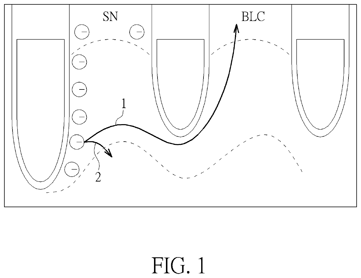
As it is shown in FIG. 1, the parasitic electron is easily induced and leaked from passgate (PG) to bit line contact (BLC) through path 1 by the repeated access to one row, thereby causing data corruption in a non-accessed physically adjacent row.
Both conditions would cause data “0” failure.
However, changing the dimensional sizes of the devices has both physical and practical limitations.
Thus, further decreasing the refresh time would cause a performance impact in the system, such as by requiring additional refresh overhead in the memory devices.

Method used


Image

  • Semiconductor structure for preventing row hammering issue in DRAM cell and method for manufacturing the same
  • Semiconductor structure for preventing row hammering issue in DRAM cell and method for manufacturing the same
  • Semiconductor structure for preventing row hammering issue in DRAM cell and method for manufacturing the same

Examples


Embodiment Construction

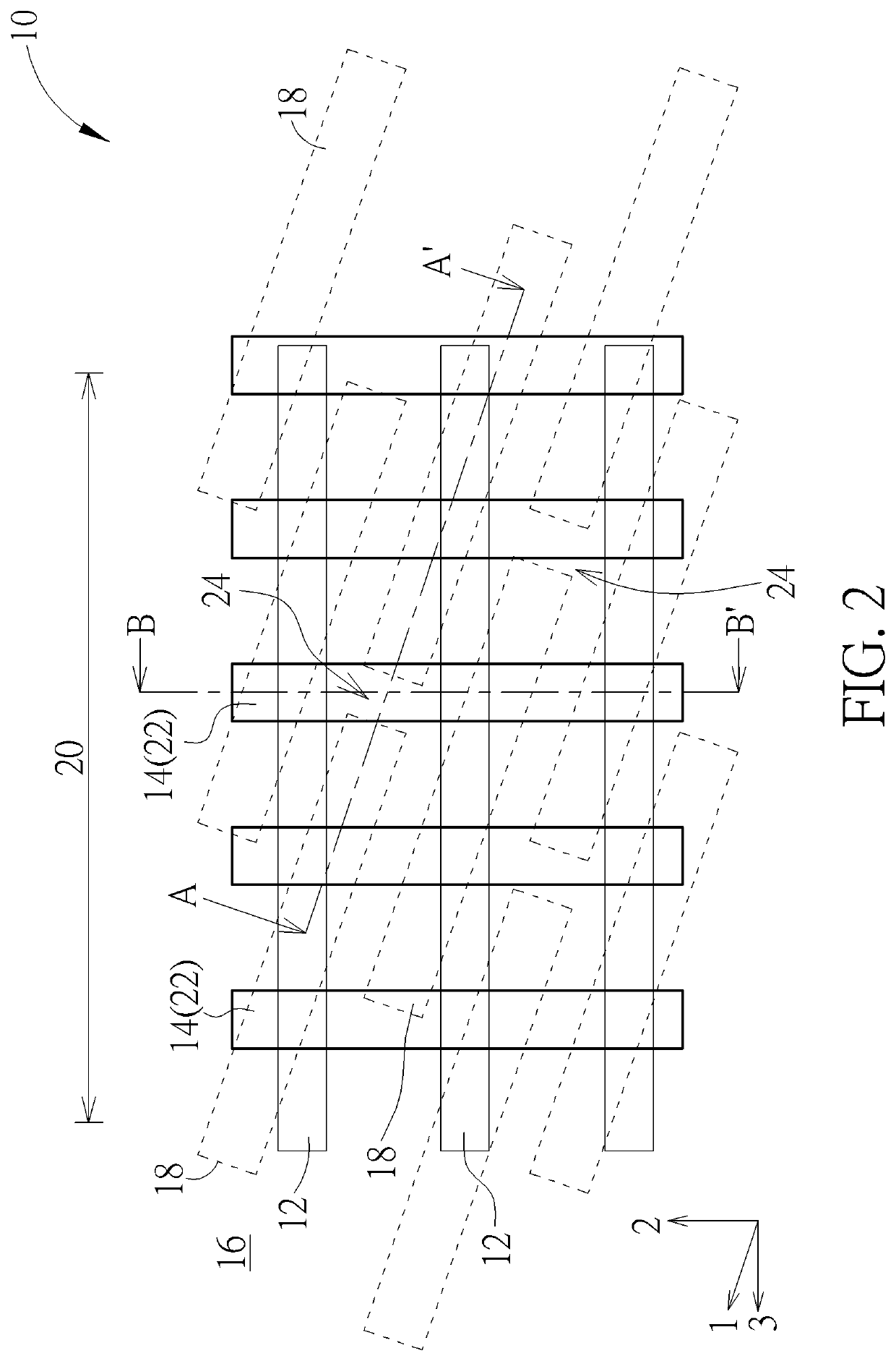
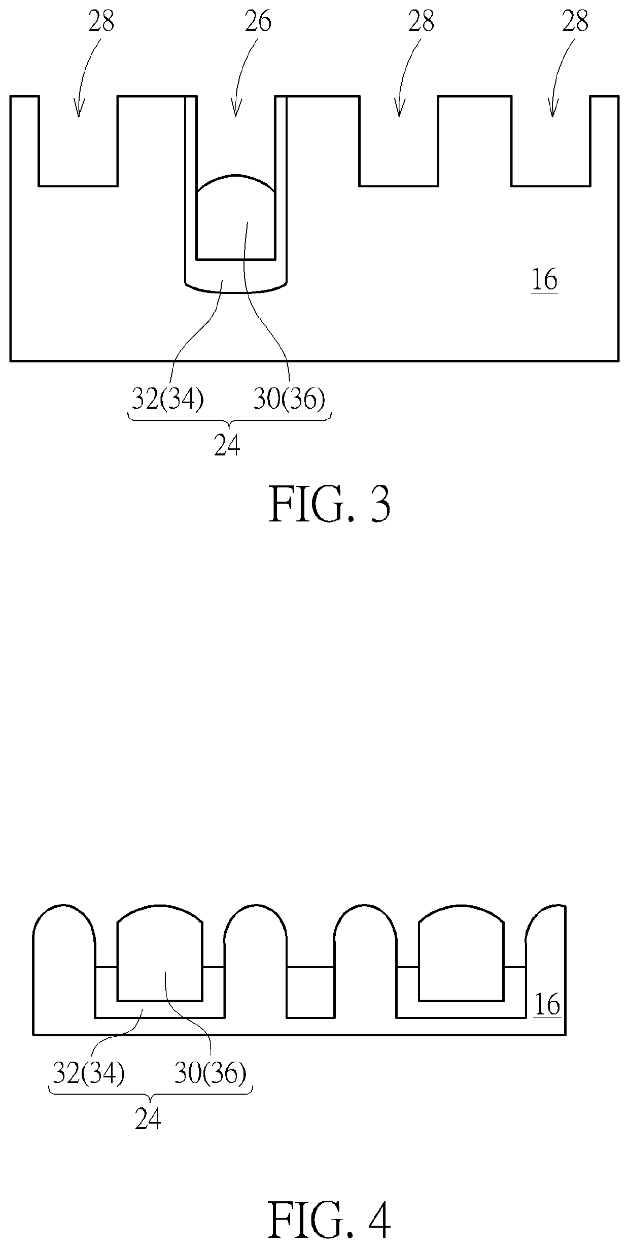
[0021]Referring to FIGS. 2-9, FIGS. 2-9 schematically illustrate a method for fabricating a DRAM device according to an preferred embodiment of the present invention, in which FIG. 2 illustrates a top-view diagram, FIG. 3 illustrates a cross-sectional view taken along the sectional line A-A′ in FIG. 2, FIG. 4 illustrates a cross-sectional view taken along the sectional line B-B′ in FIG. 1, FIG. 5 illustrates a cross-sectional view following the fabrication of FIG. 3, and FIG. 8 and FIG. 9 illustrates a cross-sectional view following the fabrication of FIG. 5 and FIG. 6, respectively. Preferably, the present embodiment pertains to the fabrication of a memory device, and more particularly a dynamic random access memory (DRAM) device 10 with buried gates, in which the DRAM device includes at least one transistor device (not shown) and at least one capacitor structure (not shown) that will be serving as a smallest constituent unit within the DRAM array and also used to receive electrica...


PUM

PropertyMeasurementUnit
angleaaaaaaaaaa
work functionaaaaaaaaaa

Abstract

A semiconductor structure for preventing row hammering issue in DRAM cell is provided in the present invention. The structure includes a trench with a gate dielectric, an n-type work function metal layer, a TiN layer conformally formed within, and a buried word line filled in the trench.

Description

CROSS REFERENCE TO RELATED APPLICATIONS[0001]This application is a divisional of application Ser. No. 15 / 627,455, filed on Jun. 20, 2017 and entitled “SEMICONDUCTOR STRUCTURE FOR PREVENTING ROW HAMMERING ISSUE IN DRAM CELL AND METHOD FOR MANUFACTURING THE SAME”, which is incorporated herein by reference.BACKGROUND OF THE INVENTION1. Field of the Invention[0002]The present invention relates generally to a semiconductor structure, and more specifically, to a semiconductor structure for preventing a row hammering issue in DRAM cells and methods for manufacturing the same.2. Description of the Prior Art[0003]With advances in computing technology, computing devices are smaller and have much more processing power. Additionally, they include more and more storage and memory to meet the needs of the programming and computing performed on the devices. The shrinking size of the devices together with the increased storage capacity is achieved by providing higher density devices, where the atom...

Claims


Application Information

Patent Timeline
Patent Type & Authority Patents(United States)
IPC IPC(8): H01L27/108H10B12/00
CPCH01L27/10814H01L27/10891H01L27/10876H01L27/10823H10B12/02H10B12/30H10B12/34H10B12/053H10B12/488H10B12/315
Inventor TSAI, CHIH-CHIEHCHEN, PIN-HONGCHEN, TZU-CHIEHCHENG, TSUN-MINCHEN, YI-WEIHUANG, HSIN-FUHSU, CHI-MAOTZOU, SHIH-FANG
Owner UNITED MICROELECTRONICS CORP
Learn More