Optical in-display fingerprint sensor and method for manufacturing such a sensor

a fingerprint sensor and optical technology, applied in the field of optical fingerprint sensing devices, can solve the problems of complex manufacturing process and sensitive to variations, and achieve the effects of increasing the distance between the transmission mask and the image sensor, maximizing the amount of light reaching the image sensor, and increasing the transmittan

Active Publication Date: 2020-08-04
FINGERPRINT CARDS ANACATUM IP AB
View PDF13 Cites 1 Cited by
  • Summary
  • Abstract
  • Description
  • Claims
  • Application Information

AI Technical Summary

Benefits of technology

[0012]According to one embodiment of the invention, the transmission mask is formed as a repeating pattern consisting of a plurality of coded aperture elements, each coded aperture element being configured to form a coded image on the image sensor. The transmission mask is thus segmented into a plurality of sub-patterns. Thereby, multiple coded images are formed on the image sensor, i.e. one for each coded aperture element, where each coded image corresponds to a portion of the fingerprint. Each coded image is individually reconstructed, and the plurality of reconstructed images are subsequently stitched together to form the final image of the fingerprint. Thereby, the computational complexity of the image reconstruction can be reduced since a lower number of pixels of the image sensor is used at each individual reconstruction.
[0019]According to one embodiment of the invention, the transmission mask may advantageously be designed based on a transmission pattern of the display panel. The transmissivity of the display panel may vary over the surface of the display panel. In particular, the display panel may have a repeating transmission pattern based on the properties o the pixel array. Since it is desirable to maximize the amount of light reaching the image sensor, the transmission mask is preferably adapted so that portions of the transmission mask with a higher proportion of openings coincide with portions of the display panel having higher transmittivity.

Problems solved by technology

However, to achieve a high-resolution sensor, the microlenses will have to be made small and be manufactured with high precision, making the manufacturing process complex and sensitive to variations, and a sensor of the described type comprising small microlenses will also be sensitive to spatial differences in transmissivity in any layer covering the sensor.

Method used


Image

  • Optical in-display fingerprint sensor and method for manufacturing such a sensor
  • Optical in-display fingerprint sensor and method for manufacturing such a sensor
  • Optical in-display fingerprint sensor and method for manufacturing such a sensor

Examples


Embodiment Construction

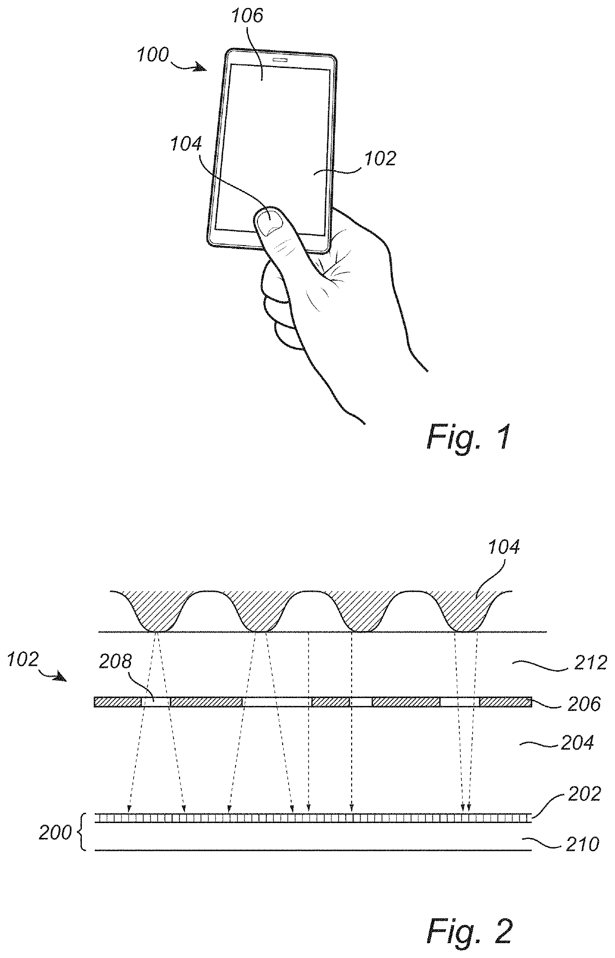
[0032]In the present detailed description, various embodiments of the optical biometric imaging device and method for manufacturing such a device according to the present invention are mainly described with reference to an optical fingerprint sensing device integrated in a display panel of a handheld device such as a smartphone. It should however be noted that the described imaging device equally well may be provided as a stand-alone device to be integrated in different applications where biometric imaging is desirable.

[0033]FIG. 1 schematically illustrates a smartphone 100 comprising an optical biometric imaging device 102 integrated in the display panel of the smartphone 100. The optical biometric imaging device 102 is configured to capture an image of an object 103 in contact with an outer surface 106 of the biometric imaging device 102. The object in contact with the outer surface 106 is here illustrated as a finger 104 in contact with the surface 106 of the display panel. In ad...


PUM


Abstract

The invention relates to an optical biometric imaging device configured to capture an image of an object in contact with an outer surface of the biometric imaging device, the biometric imaging device comprising: an image sensor comprising a photodetector pixel array; a transparent substrate arranged to cover the image sensor; a transmission mask arranged to cover the transparent substrate, wherein the transmission mask comprises a plurality of openings, the openings forming a coded aperture configured to project a coded image of an object in contact with the outer surface of the imaging device onto the image sensor; and image sensor circuitry configured to capture an image corresponding to the coded image projected onto the image sensor.

Description

CROSS REFERENCE TO RELATED APPLICATIONS[0001]This application claims priority to Swedish Application No. 1851024-8 filed on Aug. 29, 2018, the disclosure of which is incorporated herein by reference in its entirety.FIELD OF THE INVENTION[0002]The present invention relates to an optical fingerprint sensing device integrated in a display panel and to a method for manufacturing such a sensor. In particular, the invention relates to an optical fingerprint sensor comprising a coded aperture.BACKGROUND OF THE INVENTION[0003]Biometric systems are widely used as means for increasing the convenience and security of personal electronic devices, such as mobile phones etc. Fingerprint sensing systems, in particular, are now included in a large proportion of all newly released consumer electronic devices, such as mobile phones.[0004]Optical fingerprint sensors have been known for some time and may be a feasible alternative to e.g. capacitive fingerprint sensors in certain applications. Optical f...

Claims


Application Information

Patent Timeline
Patent Type & Authority Patents(United States)
IPC IPC(8): G06K9/00G06F3/042G06F3/0488G06V40/12G06V40/13
CPCG06K9/0004G06K9/00087G06F3/042G06F3/0488G06F21/32G06F2203/04103G06V40/1318G06V40/1335G06V40/1365
Inventor NILSSON, RENÉMARTINSSON, HANS
Owner FINGERPRINT CARDS ANACATUM IP AB
Why Eureka
Try Eureka