Flexible display device and method of manufacturing the same

a display device and flexible technology, applied in the field of display, can solve problems such as thin film transistor device failure, and achieve the effects of preventing crack propagation under bending stress, improving reliability of display devices, and keeping costs low

Active Publication Date: 2020-09-29
WUHAN CHINA STAR OPTOELECTRONICS SEMICON DISPLAY TECH CO LTD
View PDF8 Cites 1 Cited by
  • Summary
  • Abstract
  • Description
  • Claims
  • Application Information

AI Technical Summary

Benefits of technology

[0006]The present invention provides a flexible display device, and it can solve the problem of that a thick interlayer insulating layer is prone to crack and crack propagation under bending stress when a display is bent and causing the thin film transistor device failure.
[0020]The patterned interlayer insulating layer is used to replace the existing entire film structure, so that the channels become the deformation occurring main region when the panel is bent. Accordingly, and the reliability of the display device is improved under bending stress. Simultaneously, the thin film transistor device failure resulting from the interlayer insulating layer being crack and crack propagation under bending stress can be prevented. Also, the source and drain metal traces are used as the interlayer insulating layer and an etching mask for photoresist, so that insulating channels corresponding to the source and drain metal traces one by one can be obtained without adding a mask, and the channels can be formed in the bending stress concentration zone, and accordingly keep the cost down.

Problems solved by technology

There is a challenge to a flexible display back plate in the flexible display technology.
Currently, the flexible back plate of the flexible display device is still fabricated by using metallic and inorganic functional film layers due to limitation of materials and processes.
However, when the display device is bent, the thick interlayer insulating layer is prone to crack and crack propagation under bending stress, thereby causing the thin film transistor device failure.

Method used


Image

  • Flexible display device and method of manufacturing the same
  • Flexible display device and method of manufacturing the same
  • Flexible display device and method of manufacturing the same

Examples


Embodiment Construction

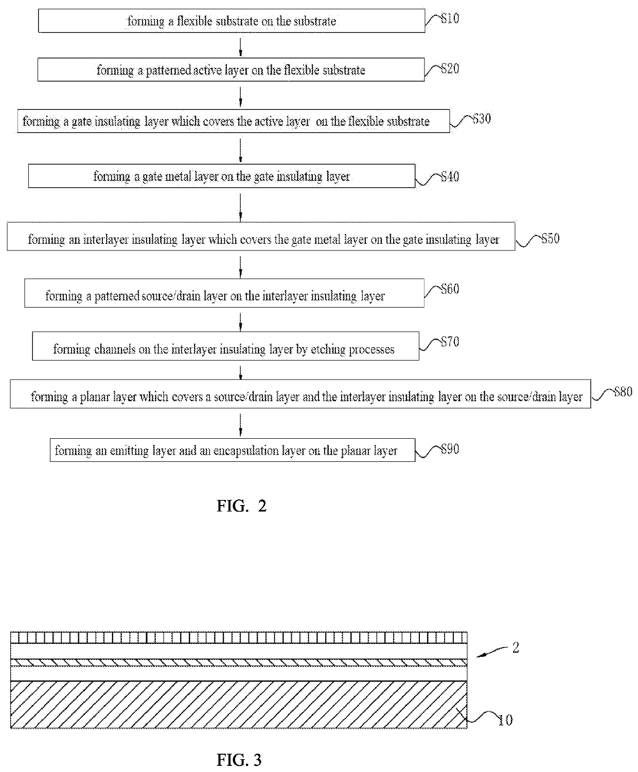
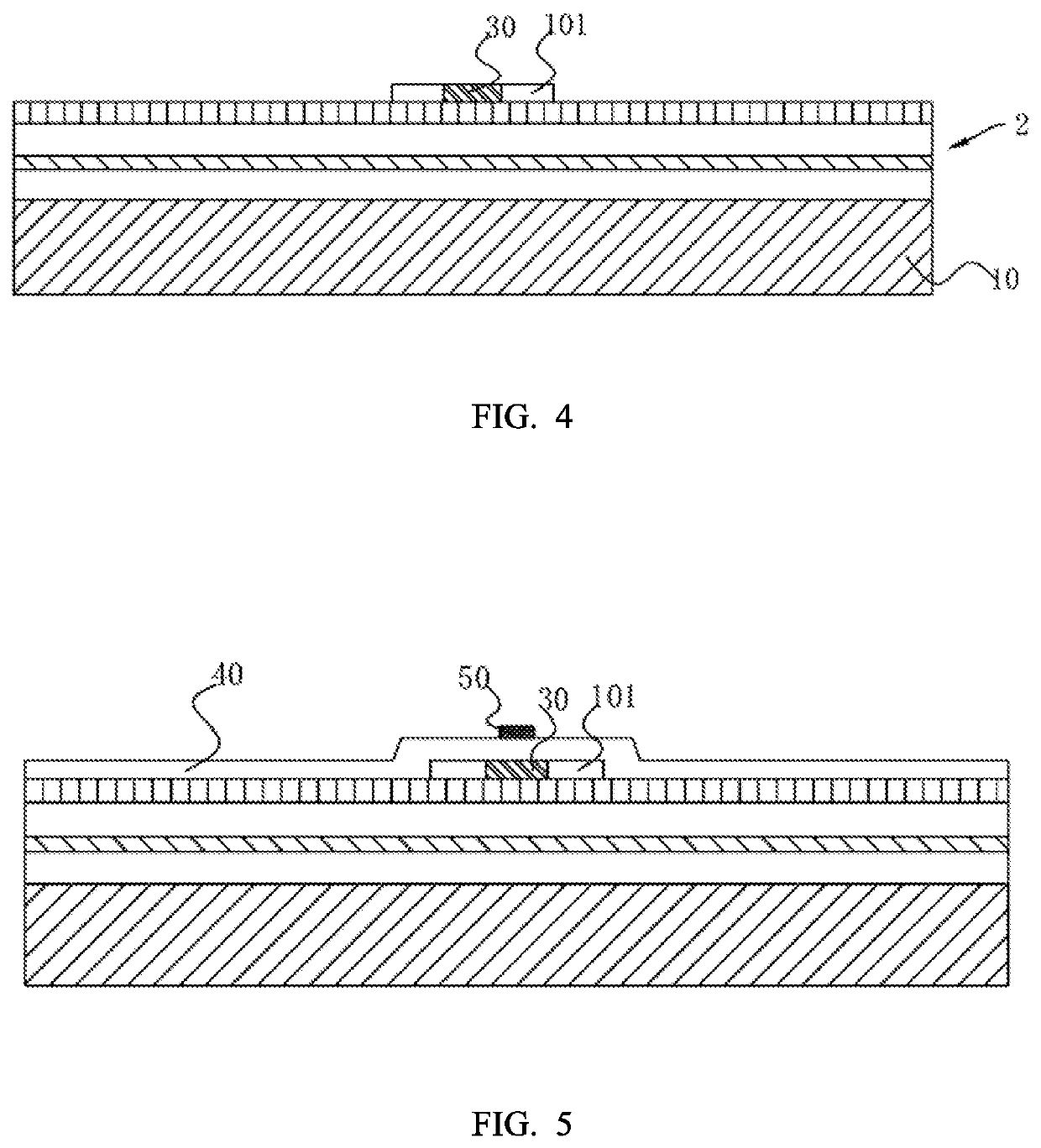
[0032]The following description of the embodiments is provided by reference to the following drawings. Directional terms mentioned in this application, such as “up,”“down,”“forward,”“backward,”“left,”“right,”“inside,”“outside,”“side,” etc., are merely indicated the direction of the drawings. Therefore, the directional terms are used for illustrating and understanding of the application rather than limiting thereof. In the figures, elements with similar structure are indicated by the same reference numerals.

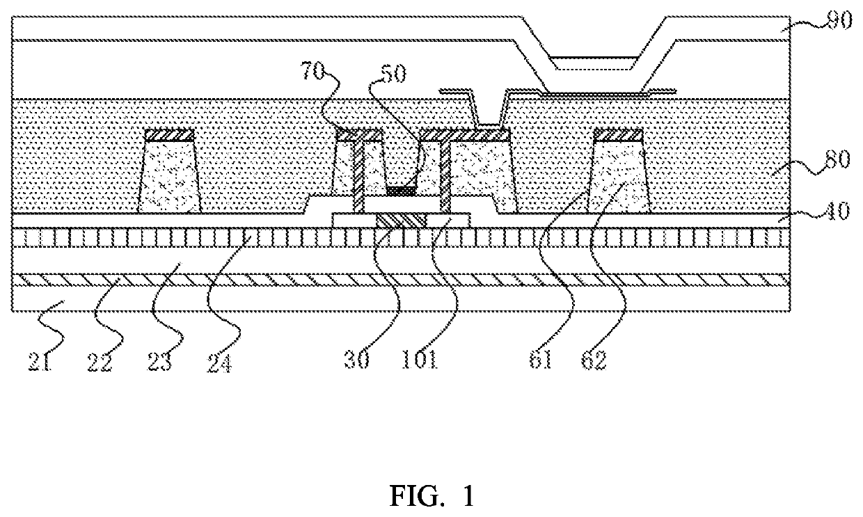
[0033]In order to achieve good insulation properties and a hydrogen replenishing effect, it is generally required that the interlayer insulating layer has a certain thickness. However, when the display device is bent, the thick interlayer insulating layer is prone to crack and crack propagation under bending stress, thereby causing the thin film transistor device failure. A flexible display device according to one embodiment of the present invention can solve above problems.

[0034]...


PUM


Abstract

A flexible display device is provided. The flexible display device comprises a flexible substrate on which an active layer, a gate insulating layer, a gate metal layer, an interlayer insulating layer, a second metal layer, a planar layer, an emitting layer and an encapsulation layer are sequentially stacked. The gate insulating layer covers the active layer, the interlayer insulating layer covers the gate metal layer and the planar layer covers the interlayer insulating layer and the second metal layer. A plurality of channels is disposed on the interlayer insulating layer, and both two ends of the channels extending toward edge of the interlayer insulating layer to penetrate the interlayer insulating layer.

Description

BACKGROUND OF THE INVENTIONField of Invention[0001]The present invention relates to a field of display, and more particularly to a field of flexible display device and a method of manufacturing thereof.Description of Prior Art[0002]A flexible display device is a display device formed based on a flexible substrate material. Since the flexible display device has the characteristics of being curved, wide viewing angle and easy to carry, the flexible display device has a broad prospect and good market potential in portable products and most display applications.[0003]There is a challenge to a flexible display back plate in the flexible display technology. The flexible display back plate requires all functional film layers to have high flexibility and reliability. Currently, the flexible back plate of the flexible display device is still fabricated by using metallic and inorganic functional film layers due to limitation of materials and processes.[0004]In the traditional flexible back pl...

Claims


Application Information

Patent Timeline
Patent Type & Authority Patents(United States)
IPC IPC(8): H01L27/12H01L27/15G09F9/30G06F1/16
CPCG09F9/301H01L27/1248H01L27/1259H01L27/1218G06F1/1652H01L27/156H01L27/1288
Inventor WANG, WEI
Owner WUHAN CHINA STAR OPTOELECTRONICS SEMICON DISPLAY TECH CO LTD
Why Eureka
Try Eureka