
Imaging device and imaging lens

a technology of imaging lens and imaging device, which is applied in the field of imaging device using an imaging lens, to achieve the effect of good balance and secure high optical performan

Active Publication Date: 2021-02-09
SONY CORP
View PDF6 Cites 0 Cited by
  • Summary
  • Abstract
  • Description
  • Claims
  • Application Information

AI Technical Summary

Benefits of technology

[0008]In PTLs 1 and 2 mentioned above, description is given of an imaging device including an imaging lens that is configured of five lenses matched with an existing high-pixel imaging element. In PTLs 1 and 2, a lens system having positive refractive power is disposed as a front group and a lens system having negative refractive power is disposed as a rear group to regulate a total optical length, and various aberrations are corrected with good balance by an aspherical lens group disposed in the rear group, thereby achieving a small, thin, and wide angle imaging device that also secures high optical performance.
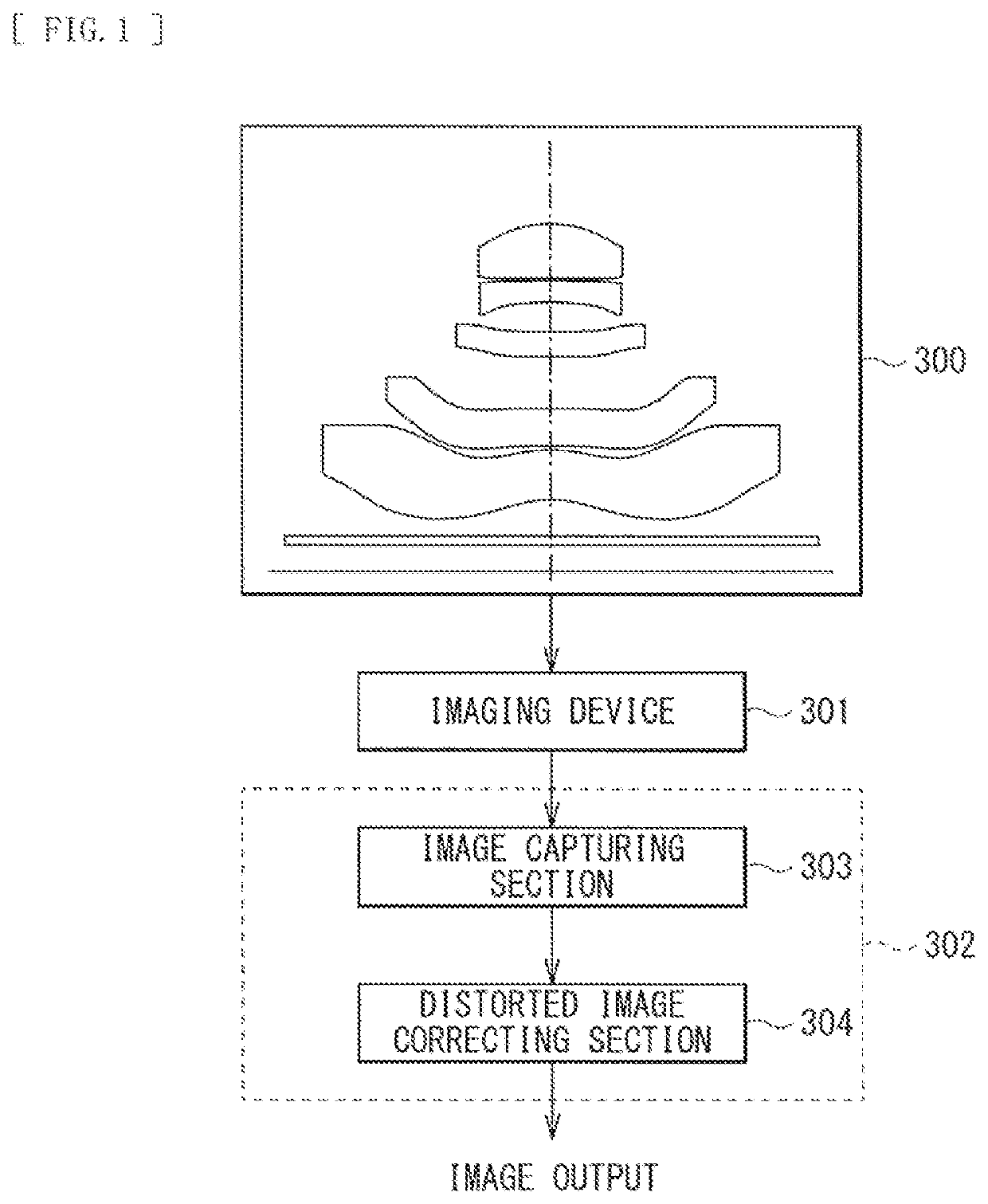
[0010]Accordingly, it is desirable to provide an imaging lens making it possible to achieve total length reduction. Further, it is desirable to provide an imaging device that corrects distortion aberration caused by the imaging lens reduced in total length, and makes it possible to achieve size reduction and thickness reduction of the entire device while securing favorable optical performance matched with a high-pixel imaging element.
[0015]In addition, in the imaging device according to the embodiment of the disclosure, the distortion aberration caused by the imaging lens reduced in total length may be corrected by the computing device.
[0016]According to the imaging lens of the embodiment of the disclosure, the power arrangement and the lens shape of the lens system are optimized, and the distortion aberration within the predetermined range are intentionally generated while the other aberrations are corrected with good balance. This makes it possible to achieve total length reduction.
[0017]Also, according to the imaging device of the embodiment of the disclosure, the distortion aberration caused by the imaging lens reduced in total length is corrected by the computing device. This makes it possible to achieve size reduction and thickness reduction of the entire device while securing favorable optical performance matched with a high-pixel imaging element.

Problems solved by technology

In contrast, such an imaging device is typically mounted with a single focus lens because of limitations of its size, and an imaging lens having a relatively wide angle of view is demanded.

Method used


Image

  • Imaging device and imaging lens
  • Imaging device and imaging lens
  • Imaging device and imaging lens

Examples


numerical example 1

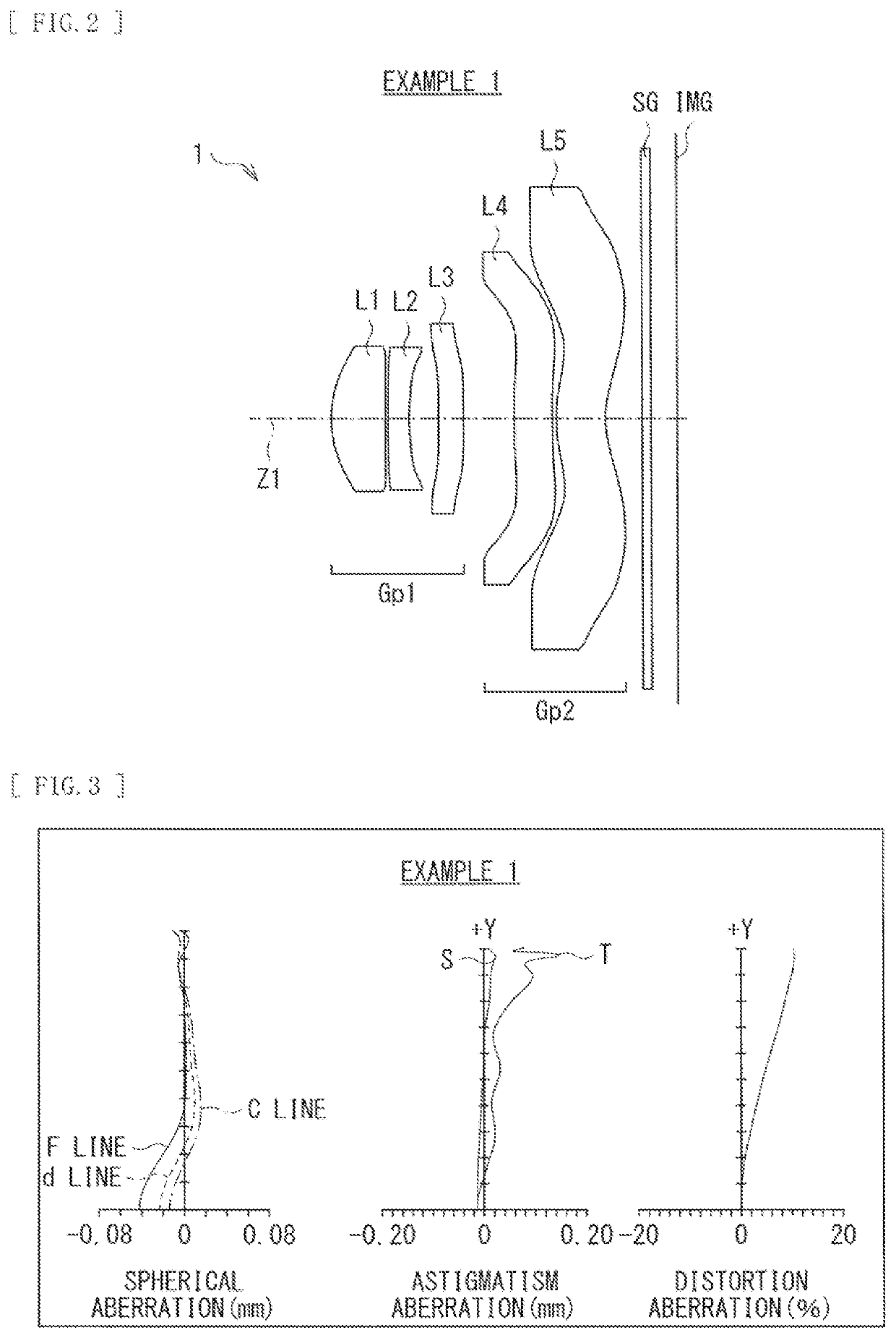
[0063]The imaging lens 1 illustrated in FIG. 2 is a lens system substantially configured of the first lens L1 to the fifth lens L5. The front-group lens system Gp1 is substantially configured of the first lens L1 to the third lens L3. The rear-group lens system Gp2 is configured of the fourth lens L4 and the fifth lens L5. The lens surface of the fifth lens L5 on the image side is concave on the image side near the optical axis, and convex on the image side around the periphery. The seal glass SG is disposed between the fifth lens L5 and the image forming surface IMG. The aperture stop is disposed in the vicinity of the front side of the first lens L1.

[0064]Table 1 shows lens data of Numerical example 1 to which specific numerical values are applied to the imaging lens 1, together with values of the focal length f of the entire lens system, the F number, and the full angle of view 2ω. In the imaging lens 1, both surfaces of each of the first lens L1 to the fifth lens L5 are aspheric...

numerical example 2

[0069]The imaging lens 2 illustrated in FIG. 4 is a lens system substantially configured of the first lens L1 to the fifth lens L5. The front-group lens system Gp1 is substantially configured of the first lens L1 to the fourth lens L4. The rear-group lens system Gp2 is configured of the fifth lens L5. The lens surface of the fifth lens L5 on the image side is concave on the image side near the optical axis, and convex on the image side around the periphery. The seal glass SG is disposed between the fifth lens L5 and the image forming surface IMG. The aperture stop is disposed in the vicinity of the front side of the first lens L1.

[0070]Table 3 shows lens data of Numerical example 2 to which specific numerical values are applied to the imaging lens 2, together with values of the focal length f of the entire lens system, the F number, and the full angle of view 2ω. In the imaging lens 2, both surfaces of each of the first lens L1 to the fifth lens L5 are aspherical. Table 4 shows valu...

numerical example 3

[0074]The imaging lens 3 illustrated in FIG. 6 is a lens system substantially configured of the first lens L1 to the fifth lens L5. The front-group lens system Gp1 is substantially configured of the first lens L1 to the third lens L3. The rear-group lens system Gp2 is configured of the fourth lens L4 and the fifth lens L5. The lens surface of the fifth lens L5 on the image side is concave on the image side near the optical axis, and convex on the image side around the periphery. The seal glass SG is disposed between the fifth lens L5 and the image forming surface IMG. The aperture stop is disposed in the vicinity of the front side of the first lens L1.

[0075]Table 5 shows lens data of Numerical example 3 to which specific numerical values are applied to the imaging lens 3, together with values of the focal length f of the entire lens system, the F number, and the full angle of view 2ω. In the imaging lens 3, both surfaces of each of the first lens L1 to the fifth lens L5 are aspheric...


PUM


Abstract

An imaging device of the disclosure includes an imaging lens; an imaging element that converts an optical image formed on an image forming surface by the imaging lens, into an electric signal; and a computing device that corrects distortion aberration of an image picked up by the imaging element. The imaging lens includes, in order from object side, a front-group lens system having positive refractive power, and a rear-group lens system having negative refractive power, a lens surface on a closest side to the image of the rear-group lens system being concave on an image side near an optical axis and convex on the image side around a periphery, and the following conditional expression is satisfied:5(%)<ODMax<20(%)  (1)where ODMax is a maximum value of distortion aberration within an imaging region of the imaging lens.

Description

CROSS REFERENCE TO RELATED APPLICATIONS[0001]This application is a U.S. National Phase of International Patent Application No. PCT / JP2014 / 076523 filed on Oct. 3, 2014, which claims priority benefit of Japanese Patent Application No. JP 2013-268398 filed in the Japan Patent Office on Dec. 26, 2013. Each of the above-referenced applications is hereby incorporated herein by reference in its entirety.TECHNICAL FIELD[0002]The disclosure relates to an imaging device using an imaging lens. More specifically, the disclosure relates to an imaging device that provides high image quality and has small thickness, and is suitable for a small imaging device using a solid-state imaging element such as a CMOS, for example, a mobile phone with a camera, and to an imaging lens used in such an imaging device.BACKGROUND ART[0003]Mobile phones with cameras and digital still cameras are known, using solid-state imaging element such as a charge coupled device (CCD) and a complementary metal-oxide semicond...

Claims


Application Information

Patent Timeline
Patent Type & Authority Patents(United States)
IPC IPC(8): G06T5/00G02B27/00G02B13/00
CPCG06T5/006G02B13/004G02B13/0045G02B27/0025
Inventor NIHEI, YASUHIDETAMURA, MASAKINABETA, KENSHIKATSURAGI, DAIGO
Owner SONY CORP
Learn More