Insulated gate power semiconductor device and method for manufacturing such a device

a technology of insulated gate and semiconductor, which is applied in the field of power electronics, can solve the problems of reducing the efficiency affecting the performance of the blocking layer, and affecting the performance of the enhancement layer, and achieves the effects of simple, cheap and fast manufacturing methods, and adding delicate manufacturing steps

Active Publication Date: 2021-07-27
HITACHI ENERGY LTD
View PDF17 Cites 0 Cited by
  • Summary
  • Abstract
  • Description
  • Claims
  • Application Information

AI Technical Summary

Benefits of technology

[0018]It is an object of the invention to provide a power semiconductor device, which simultaneously has low on-state losses and high breakdown voltage, compared to prior art devices and which device is manufactured by an easy and fast manufacturing method avoiding delicate manufacturing steps.

Problems solved by technology

However, such a prior art device having a highly doped enhancement layer 95 will suffer from worse SOA and breakdown voltage compared to standard trench IGBTs.
Practical enhancement layer doping concentrations are therefore limited to values smaller than 2.5*1016 cm−3 to prevent excessive electric fields and therefore degradation of the blocking performance and turn-off SOA.
Nevertheless, the introduction of p doped protection pillows 8 at the trench bottoms 76 improves the device robustness, being able to postpone the onset of the breakdown mechanism, but is not able to redeem the inherent weakness of a trench IGBT device sufficiently where the impact ionization is caused by increased enhancement doping concentration.
This potentially translates in unwanted drawbacks such as hot carrier injection in the gate oxide with consequent threshold voltage instabilities.
Eventually, this device also shows a degraded dynamic avalanche robustness, and this phenomena is even more exacerbated under hard switching conditions.
In a prior art trench IGBT with enhancement layer, the enhancement layer may lead to premature device failure (breakdown).
However, such layered structures are laborious to form.
However the weakness of avalanche generation at the enhancement / channel interface is present in the prior art device 4 (FIG. 20) with increased ND,enh.
Thus, such a semiconductor device provides no MOS or IGBT functionality.

Method used


Image

  • Insulated gate power semiconductor device and method for manufacturing such a device
  • Insulated gate power semiconductor device and method for manufacturing such a device
  • Insulated gate power semiconductor device and method for manufacturing such a device

Examples


Embodiment Construction

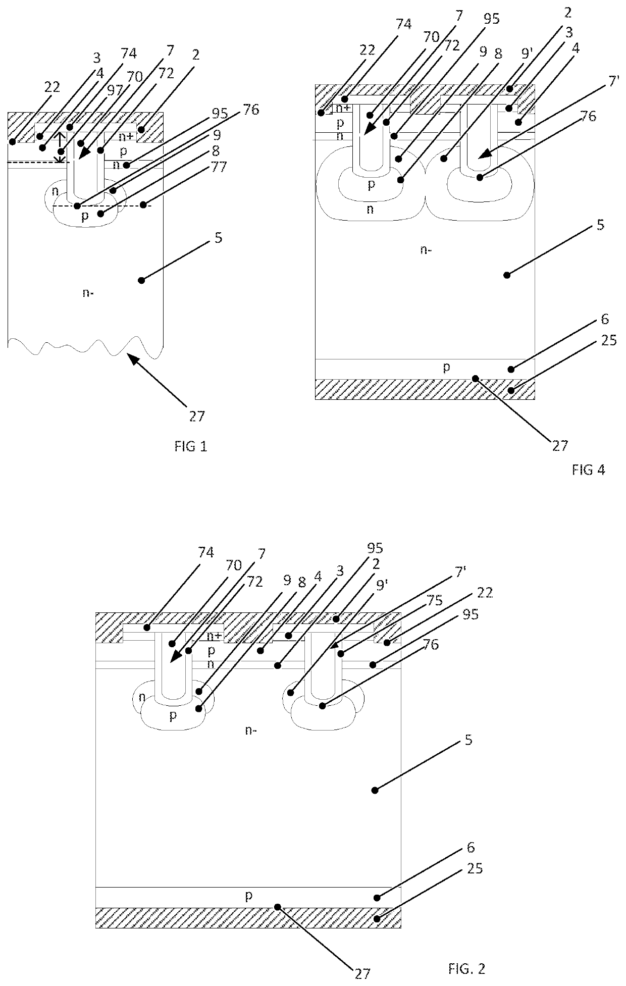
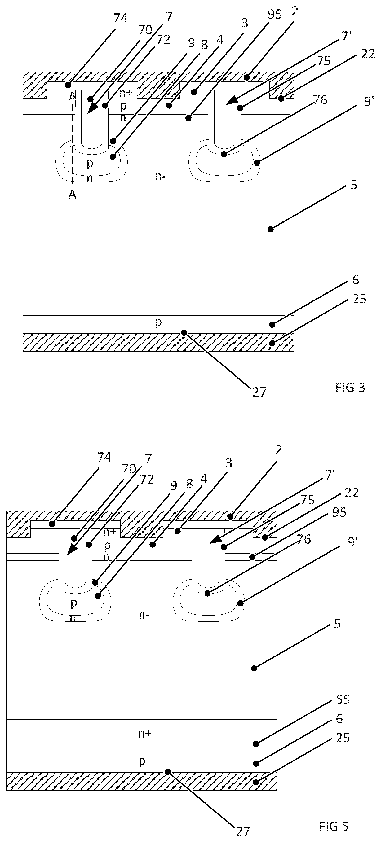
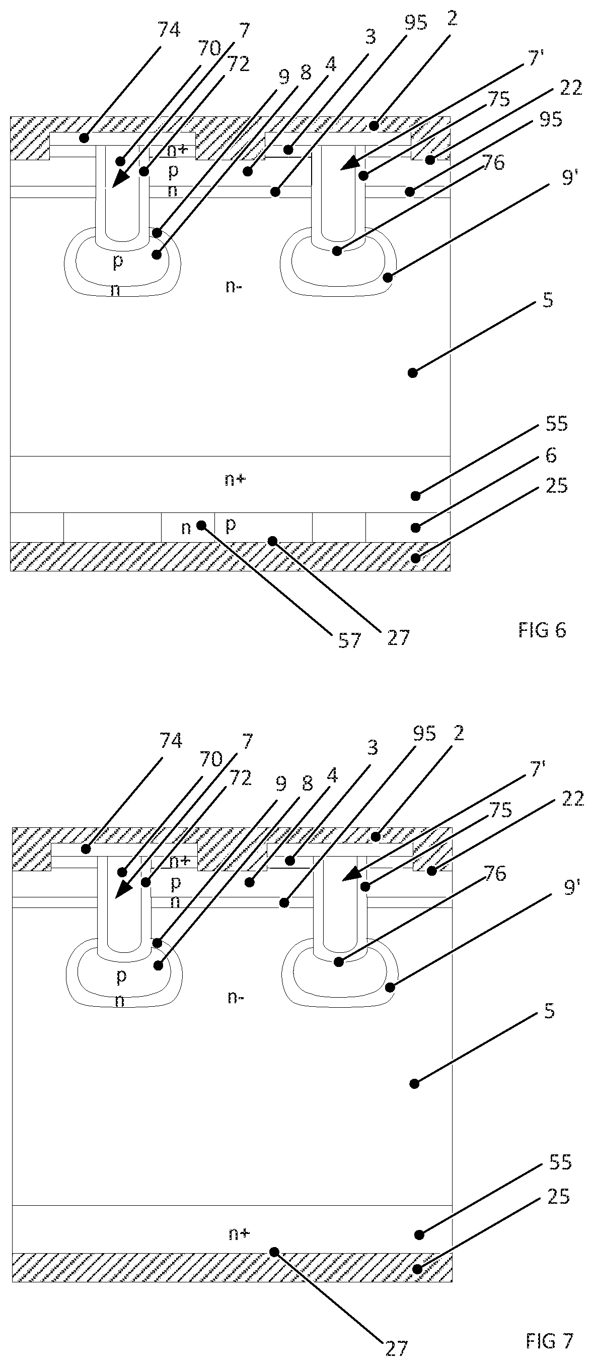
[0047]In FIG. 1 a structure on an emitter side 22 for an inventive insulated gate power semiconductor device is shown. The device comprises an emitter electrode 2 on an emitter side 22 and a collector electrode 25 on a collector side 27, which collector side 27 is arranged opposite to the emitter side 22. An (n−) doped drift layer 5 is arranged between the emitter side 22 and the collector side 27. A p doped base layer 4 is arranged between the drift layer 5 and the emitter side 22. The base layer 4 contacts the emitter electrode 2. An n doped source layer 3 having higher doping concentration than the drift layer is also arranged on the emitter side 22. The source layer 3, which is separated from the drift layer 5 by the base layer 4, contacts the emitter electrode 2. The source layer 3 may be arranged such that the source layer 3 is arranged at both sides of each gate electrode 7, 7′.

[0048]The doping concentration of the base layer 4 and the drift layer 5 can be freely chosen due t...


PUM

PropertyMeasurementUnit
thicknessaaaaaaaaaa
thicknessaaaaaaaaaa
thicknessaaaaaaaaaa

Abstract

An insulated gate power semiconductor device includes an (n-) doped drift layer between an emitter side and a collector side. A p doped protection pillow covers a trench bottom of a trench gate electrode. An n doped enhancement layer having a maximum enhancement layer doping concentration in an enhancement layer depth separates the base layer from the drift layer. An n doped plasma enhancement layer having a maximum plasma enhancement layer doping concentration covers an edge region between the protection pillow and the trench gate electrode. The N doping concentration decreases from the maximum enhancement layer doping concentration towards the plasma enhancement layer and the N doping concentration decreases from the maximum plasma enhancement layer doping concentration towards the enhancement layer such that the N doping concentration has a local doping concentration minimum between the enhancement layer and the plasma enhancement layer.

Description

TECHNICAL FIELD[0001]The invention relates to the field of power electronics, and more particularly to a device as such according to the preamble of the independent claim 1 or to a method for manufacturing an insulated gate power semiconductor device according to the independent claim 12.BACKGROUND ART[0002]In FIG. 18 a prior art insulated gate bipolar transistor (IGBT) is shown as known from EP 0 795 911 A2. The prior art device comprises an active cell with layers of different conductivity types in the following order between an emitter electrode 2 on an emitter side 22 and a collector electrode 25 on a collector side 27 opposite to the emitter side 22: an (n+) doped source layer 3, a p doped base layer 4, which contacts the emitter electrode 2, an n doped enhancement layer 95, an (n−) doped drift layer 5, an (n+) doped buffer layer 55 and a p doped collector layer 6.[0003]A trench gate electrode 7 is arranged on the emitter side 22, which comprises a gate layer 70 and a first ele...

Claims


Application Information

Patent Timeline
Patent Type & Authority Patents(United States)
IPC IPC(8): H01L29/66H01L29/739H01L29/06H01L29/10H01L29/78H01L21/225H01L21/265H01L29/08H01L21/266
CPCH01L29/66734H01L29/0619H01L29/0623H01L29/0834H01L29/10H01L29/66348H01L29/7397H01L29/7813H01L21/2253H01L21/266H01L21/26513
Inventor DE-MICHIELIS, LUCACORVASCE, CHIARA
Owner HITACHI ENERGY LTD
Why Eureka
Try Eureka