Method and circuit for reducing losses in DC-DC converters

a dc-dc converter and loss reduction technology, applied in the field of integrated circuits, can solve the problems of large dynamic loss, slow control signal rise and fall times, and dominant loss of gate capacitance switching, so as to reduce dynamic loss, reduce conduction loss, and reduce dynamic and conduction loss. the effect of independent reduction

Inactive Publication Date: 2005-08-16
SEMICON COMPONENTS IND LLC
View PDF43 Cites 45 Cited by
  • Summary
  • Abstract
  • Description
  • Claims
  • Application Information

AI Technical Summary

Benefits of technology

[0006]In accordance with the present invention, a switching converter includes two transistors Q1 and Q2 parallel-connected between two terminals. Transistor Q1 is optimized to reduce the dynamic loss and transistor Q2 is optimized to reduce the conduction loss. Q1 and Q2 are configured and operated such that the dynamic loss of the converter is dictated substantially by Q1 and the conduction loss of the converter is dictated substantially by Q2. Thus, the tradeoff between these two types of losses present in conventional techniques is eliminated, allowing the dynamic and conduction losses to be independently reduced. Further, the particular configuration and manner of operation of Q1 and Q2 enable reduction of the gate capacitance switching loss when operating under low load current conditions.

Problems solved by technology

However, the gate capacitance switching loss becomes dominant at lower load currents.
Larger MOSFETs, however, have larger gate charge Qg leading to slower control signal rise and fall times and therefore larger dynamic loss.
Conversely, in order to reduce the dynamic loss, it is desirable to reduce the gate charge Qg which requires smaller MOSFETs which in result in increased RDSon and therefore increased conduction loss.
This trade-off has forced conventional designs to compromise between the two types of losses resulting in a less than optimum design in terms of efficiency.

Method used


Image

  • Method and circuit for reducing losses in DC-DC converters
  • Method and circuit for reducing losses in DC-DC converters
  • Method and circuit for reducing losses in DC-DC converters

Examples


Embodiment Construction

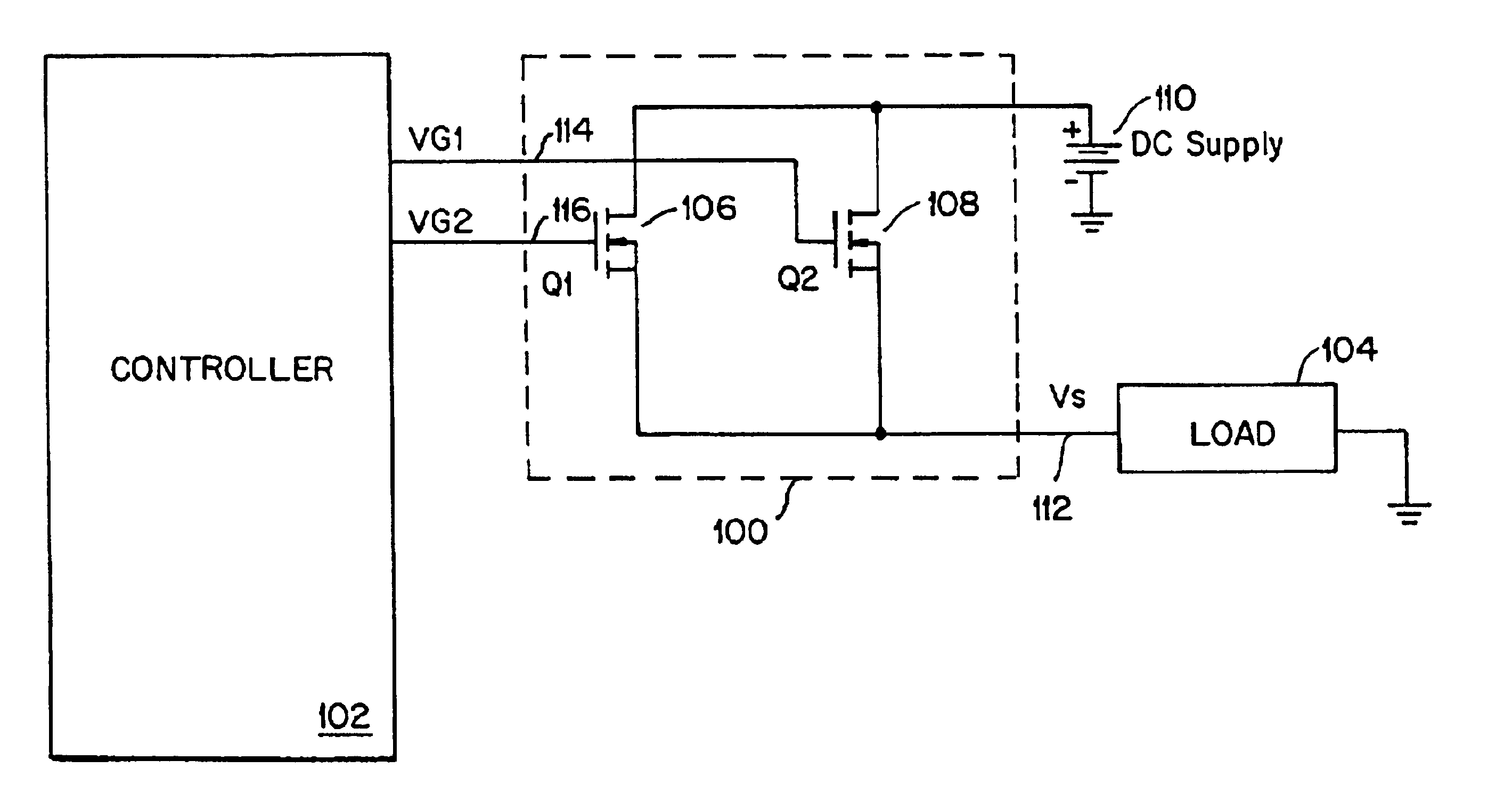
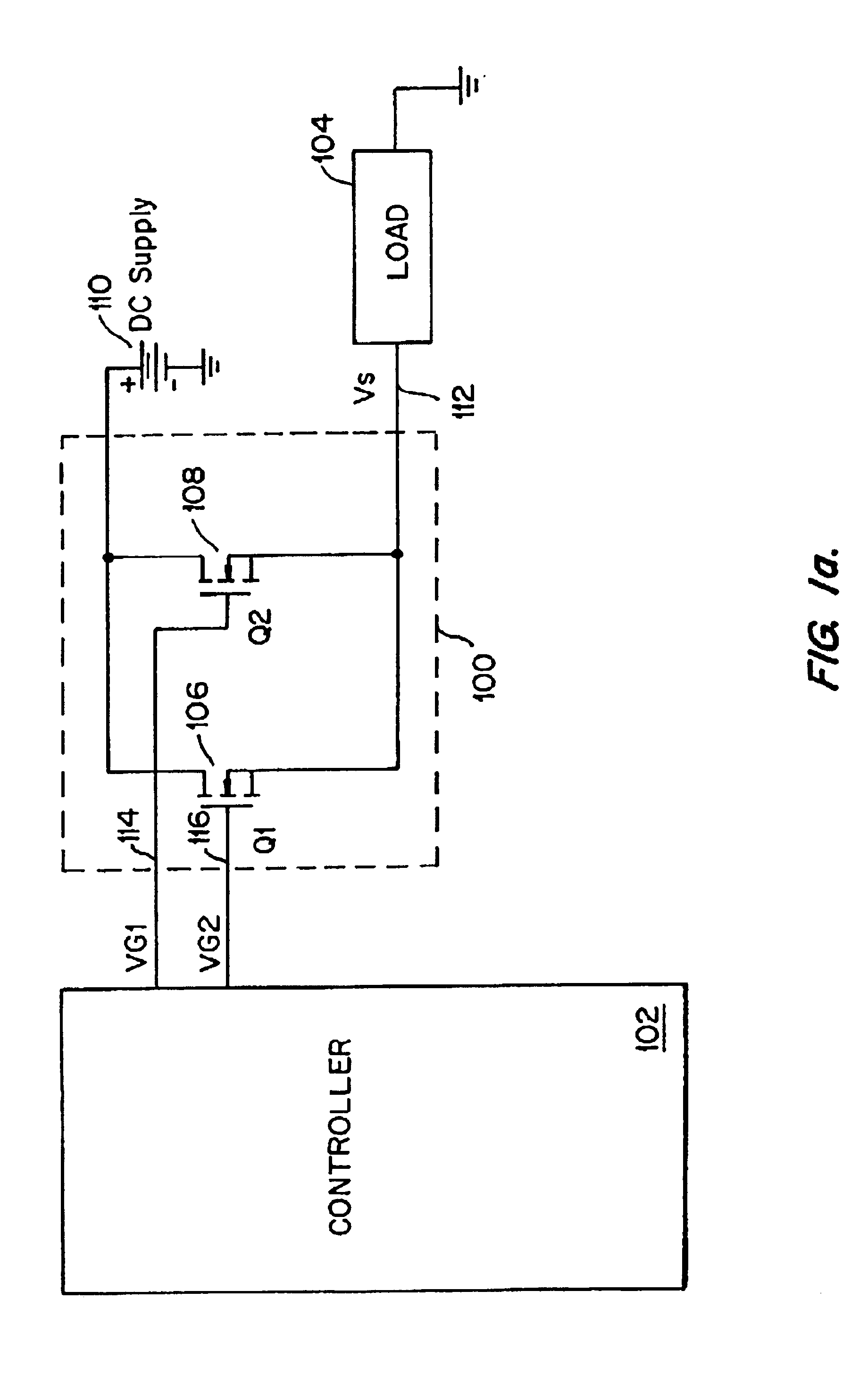
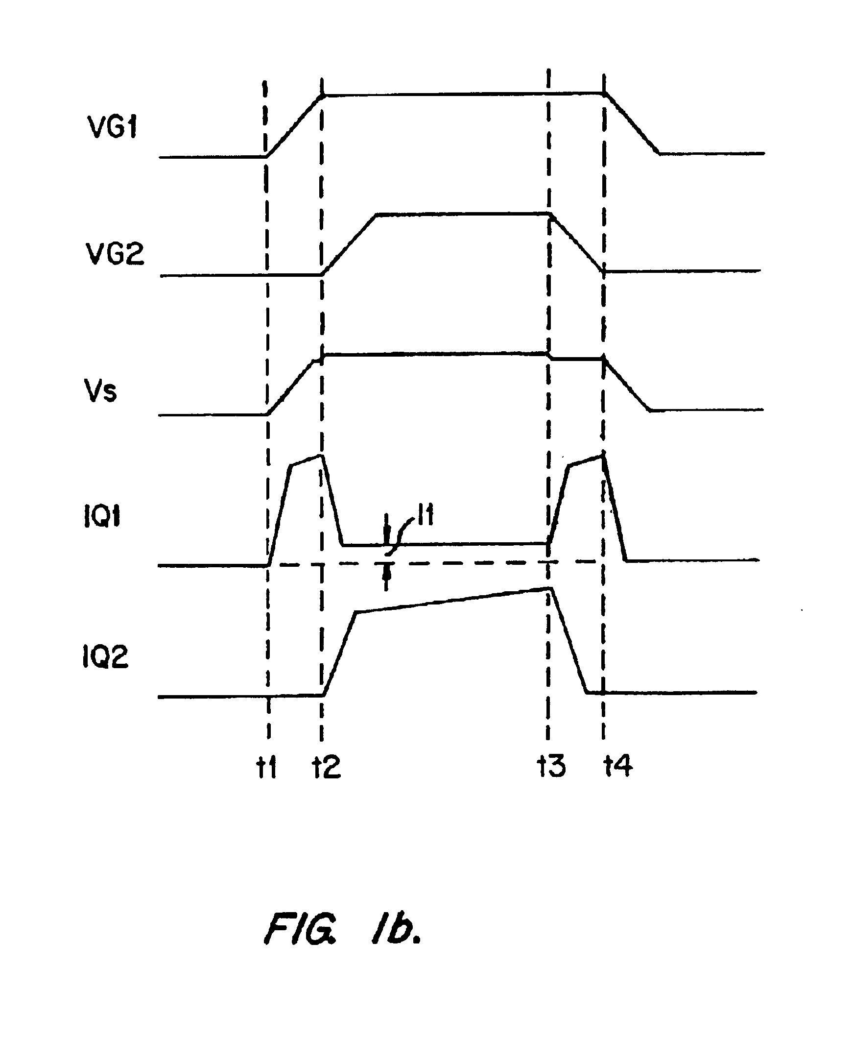
[0030]In accordance with the present invention, a method and circuitry for implementing switching converters that improve switching efficiency by reducing the conduction loss, the dynamic loss, and the gate capacitance switching loss are provided. The switching converter includes two transistors Q1 and Q2 parallel-connected between two terminals. Transistor Q1 is optimized to reduce the dynamic loss and transistor Q2 is optimized to reduce the conduction loss. Q1 and Q2 are configured and operated such that the dynamic loss of the converter is dictated substantially by Q1 and the conduction loss of the converter is dictated substantially by Q2. Thus, the tradeoff between these two types of losses present in conventional techniques is eliminated, allowing the dynamic and conduction losses to be independently reduced. Further, the particular configuration and manner of operation of Q1 and Q2 enable reduction of the gate capacitance switching loss when operating under low load current ...


PUM


Abstract

In accordance with the present invention, a switching converter includes two transistors Q1 and Q2 parallel-connected between two terminals. Transistor Q1 is optimized to reduce the dynamic loss and transistor Q2 is optimized to reduce the conduction loss. Q1 and Q2 are configured and operated such that the dynamic loss of the converter is dictated substantially by Q1 and the conduction loss of the converter is dictated substantially by Q2. Thus, the tradeoff between these two types of losses present in conventional techniques is eliminated, allowing the dynamic and conduction losses to be independently reduced. Further, the particular configuration and manner of operation of Q1 and Q2 enable reduction of the gate capacitance switching loss when operating under low load current conditions.

Description

CROSS-REFERENCES TO RELATED APPLICATIONS[0001]This application claims priority from U.S. application No. 60 / 314,607, filed Aug. 23, 2001, entitled “Method and Circuit for Reducing Losses in DC-DC Converters”, which disclosure is incorporated by reference.BACKGROUND OF THE INVENTION[0002]The present invention relates in general to integrated circuits, and in particular to method and circuitry for implementing more efficient DC-DC converters.[0003]One type of DC-DC converter employs transistor switches that are controlled to periodically transfer charge from an input DC voltage supply to a load device across which the output DC voltage is established. Although there are different ways to realize this type of switching conversion, the most common technique uses inductors and capacitors as energy storage elements and one or more MOSFETs as the switching elements.[0004]To increase the efficiency of the converter, attempts are made to minimize the losses in the switching elements (MOSFETs...

Claims


Application Information

Patent Timeline
Patent Type & Authority Patents(United States)
IPC IPC(8): H03K17/687H02M3/158H02M3/04H03K17/12H03K17/00H02M3/155H02M3/28
CPCH02M3/1584H03K17/6871H03K17/122H03K2217/0036
Inventor ELBANHAWY, ALAN
Owner SEMICON COMPONENTS IND LLC
Why Eureka
Try Eureka