Electromagnetic wave absorber

a technology of electromagnetic absorbers and absorbers, which is applied in the field of electromagnetic absorbers, can solve the problems of inability to provide sufficient absorption performance at a set frequency, inability to cover high frequency bands, and limited range of conventional electromagnetic absorbers, so as to achieve uniform electromagnetic wave absorbing effect, widen absorption bandwidth, and widen absorption bandwidth

Active Publication Date: 2021-10-12
NITTO DENKO CORP
View PDF32 Cites 1 Cited by
  • Summary
  • Abstract
  • Description
  • Claims
  • Application Information

AI Technical Summary

Benefits of technology

[0007]In view of the foregoing, it is therefore an object of the present invention to provide an electromagnetic wave absorber usable for radar having a high resolution and having excellent absorption performance over a wide bandwidth.
[0014]In particular, the electromagnetic wave absorber comprising: a dielectric layer; a resistive layer provided on a first surface of the dielectric layer; and an electrically conductive layer provided on a second surface of the dielectric layer and having a sheet resistance lower than that the resistive layer, wherein the dielectric layer has a relative dielectric constant in the range of 1 to 10 is capable of not only widening the absorption bandwidth but also providing the dielectric layer having an easy-to-control thickness. This provides the electromagnetic wave absorber having a more uniform electromagnetic wave absorbing effect.
[0015]Also, the electromagnetic wave absorber comprising: a dielectric layer; and an electrically conductive layer provided on one surface of the dielectric layer, wherein the dielectric layer has a relative dielectric constant in the range of 1 to 10 is capable of not only widening the absorption bandwidth but also facilitating the setting and manufacture thereof. This achieves the electromagnetic wave absorber at low costs.

Problems solved by technology

Unfortunately, conventional electromagnetic wave absorbers have problems in being able to provide absorption performance only in a very limited range close to a target frequency and in being unable to cover high frequency bands, as disclosed in PTL 1 and PTL 2.
This results in apprehension that sufficient absorption performance cannot be provided at a set frequency.
Another problem lies in that the electromagnetic wave absorber fails to provide absorption performance if the radar frequency is varied even slightly.
However, the absorption performance of the electromagnetic wave absorbers is provided only in a very limited range close to a target frequency, as described above.
This gives rise to problems of the increased costs of the electromagnetic wave absorbers and the increased gross weight due to the use of the multiplicity of electromagnetic wave absorbers.

Method used


Image

  • Electromagnetic wave absorber
  • Electromagnetic wave absorber
  • Electromagnetic wave absorber

Examples


##ventive example 1

Inventive Example 1

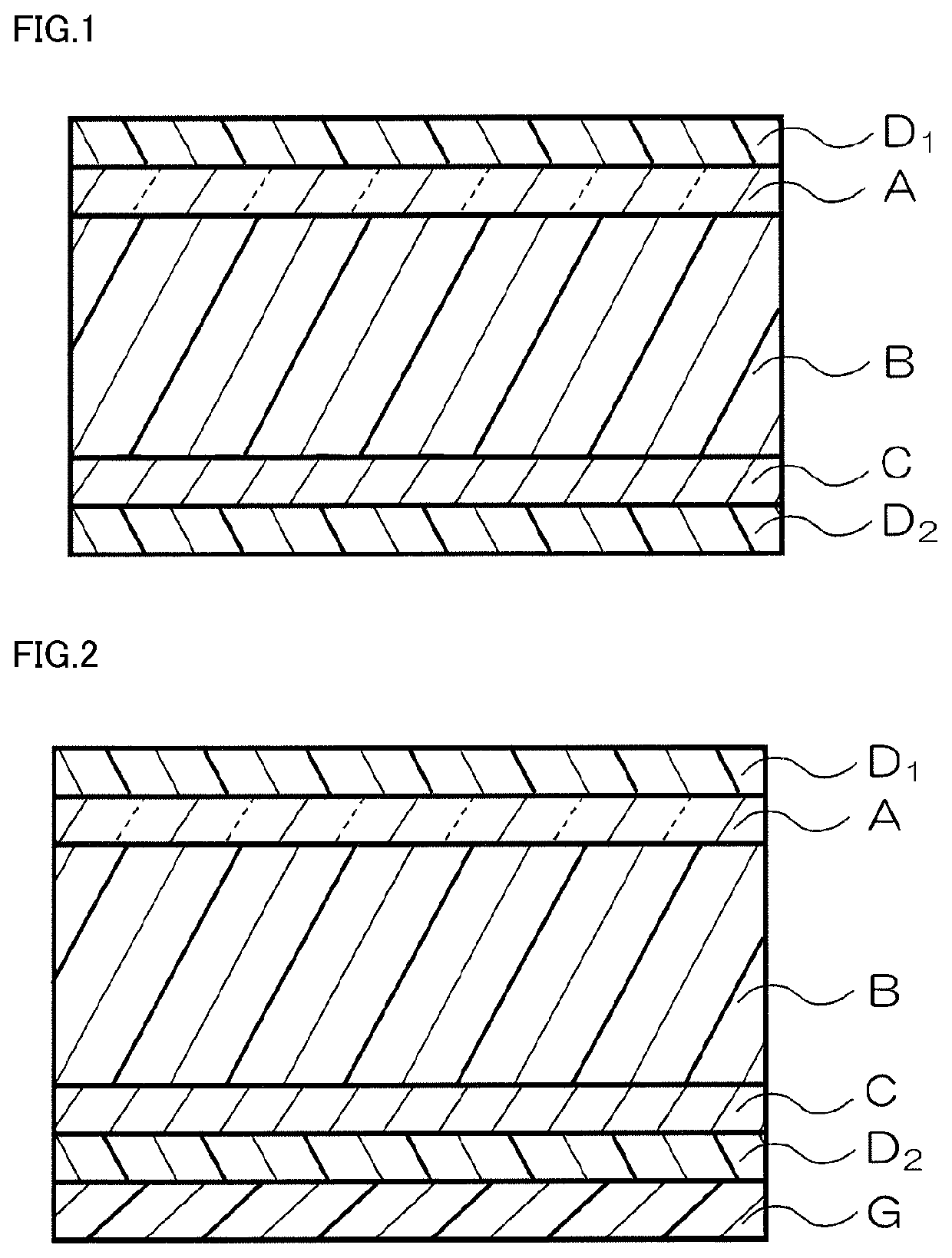
[0058]Pursuant to the method of providing the electromagnetic wave absorber shown in FIG. 1, an EVA resin (Evaflex EV250, with a relative dielectric constant of 2.45) available from Du Pont-Mitsui Polychemicals Co., Ltd. was pressed at 120° C. into a film having a thickness of 560 μm. Thus, the dielectric layer B was produced. A PET film (resin layer D1) having a thickness of 38 μm on which ITO serving as the electrically conductive layer C was sputtered so as to have a surface resistance of 20Ω / □ was affixed to a second surface of the dielectric layer B so that the electrically conductive layer C faced the dielectric layer B. A PET film (resin layer D2) having a thickness of 38 μm on which. ITO serving as the resistive layer A was sputtered so as to have a surface resistance of 380Ω / □ was affixed to a first surface of the dielectric layer B so that the resistive layer A faced the dielectric layer B. Thus, an intended electromagnetic wave absorber was provided.

##ventive example 2

Inventive Example 2

[0059]Pursuant to the method of providing the electromagnetic wave absorber shown in FIG. 1, an intended electromagnetic wave absorber was provided in substantially the same manner as in Inventive Example 1 except that the dielectric layer B was changed to that to be described below.

[0060](Dielectric Layer B)

[0061]The dielectric layer B was produced by adding 50 parts by weight of barium titanate (BT-01) available from Sakai Chemical Industry Co., Ltd. to 100 parts by weight of an EVA resin (Evaflex EV250) available from Du Pont-Mitsui Polychemicals Co., Ltd.; kneading the resulting mixture in a mixing mill; and then pressing the kneaded mixture at 120° C. into a film having a thickness of 458 μm. The dielectric layer B had a relative dielectric constant of 3.90.

##ventive example 3

Inventive Example 3

[0062]Pursuant to the method of providing the electromagnetic wave absorber shown in FIG. 1, an intended electromagnetic wave absorber was provided in substantially the same manner as in Inventive Example 1 except that the dielectric layer B was changed to that to be described below.

[0063](Dielectric Layer B)

[0064]The dielectric layer B was produced by adding 100 parts by weight of barium titanate (BT-01) available from Sakai Chemical Industry Co. Ltd. to 100 parts by weight of an EVA resin (Evaflex EV250) available from Du Pont-Mitsui Polychemicals Co, Ltd.; kneading the resulting mixture in a mixing mill; and then pressing the kneaded mixture at 120° C. into a film having a thickness of 397 μm. The dielectric layer B had a relative dielectric constant of 5.19.


PUM

PropertyMeasurementUnit
relative dielectric constantaaaaaaaaaa
thicknessaaaaaaaaaa
frequencyaaaaaaaaaa

Abstract

For the purpose of providing an electromagnetic wave absorber usable for radar having a high revolution and sufficiently adaptable to a plurality of radars different in frequency, the bandwidth of a frequency band in which an electromagnetic wave absorption amount is not less than 20 dB is not less than 2 GHz, within a frequency band of 60 to 90 GHz.

Description

TECHNICAL FIELD[0001]The present invention relates to an electromagnetic wave absorber for preventing electromagnetic interference.BACKGROUND ART[0002]In recent years, the use of electromagnetic waves as an information communication medium has been on the increase. Examples the use of such electromagnetic waves include collision avoidance systems in the field of motor vehicle technology. The collision avoidance systems automatically apply brakes upon sensing obstacles by means of radar, and measure the speed of a neighboring vehicle and a distance between a user's vehicle and the neighboring vehicle to control the speed of the user's vehicle and the distance between the vehicles. For normal operation of the collision avoidance systems and the like, it is important to receive as little unwanted electromagnetic wave radiation (noise) as possible in order to prevent false recognition. For this reason, electromagnetic wave absorbers that absorb noise are sometimes used in these systems ...

Claims


Application Information

Patent Timeline
Patent Type & Authority Patents(United States)
IPC IPC(8): H01Q17/00B32B27/30B32B27/08B32B15/08B32B33/00B32B7/12H05K9/00B32B27/28H01Q1/32B32B27/18G01S13/931B32B15/20
CPCH01Q17/00B32B7/12B32B27/08B32B27/18B32B27/28B32B27/30B32B27/304B32B27/306H01Q1/3283H05K9/00H05K9/0088H05K9/0094B32B15/08B32B15/20B32B33/00B32B2255/06B32B2255/10B32B2255/205B32B2264/102B32B2264/105B32B2307/202B32B2307/204B32B2307/40B32B2457/00G01S13/931B32B7/02B32B27/00H05K9/0084B32B9/045B32B2307/206B32B2307/212
Inventor UKEI, HIROICHIUI, TAKEHIROYAMAGATA, KAZUTOTAKEDA, YUKIMACHINAGA, HIRONOBUKITAGAWA, YUYASASA, KAZUAKI
Owner NITTO DENKO CORP
Why Eureka
Try Eureka