Wiring board manufacturing method
a manufacturing method and wiring technology, applied in the direction of electrical equipment, printed circuits, electrical components, etc., can solve the problems of small distance between electrodes on each package device chip, variation in the height of the wiring layer, and the inability to apply copper-clad laminates to such a case. , to achieve the effect of suppressing poor connection
- Summary
- Abstract
- Description
- Claims
- Application Information
AI Technical Summary
Benefits of technology
Problems solved by technology
Method used
Image
Examples
first preferred embodiment
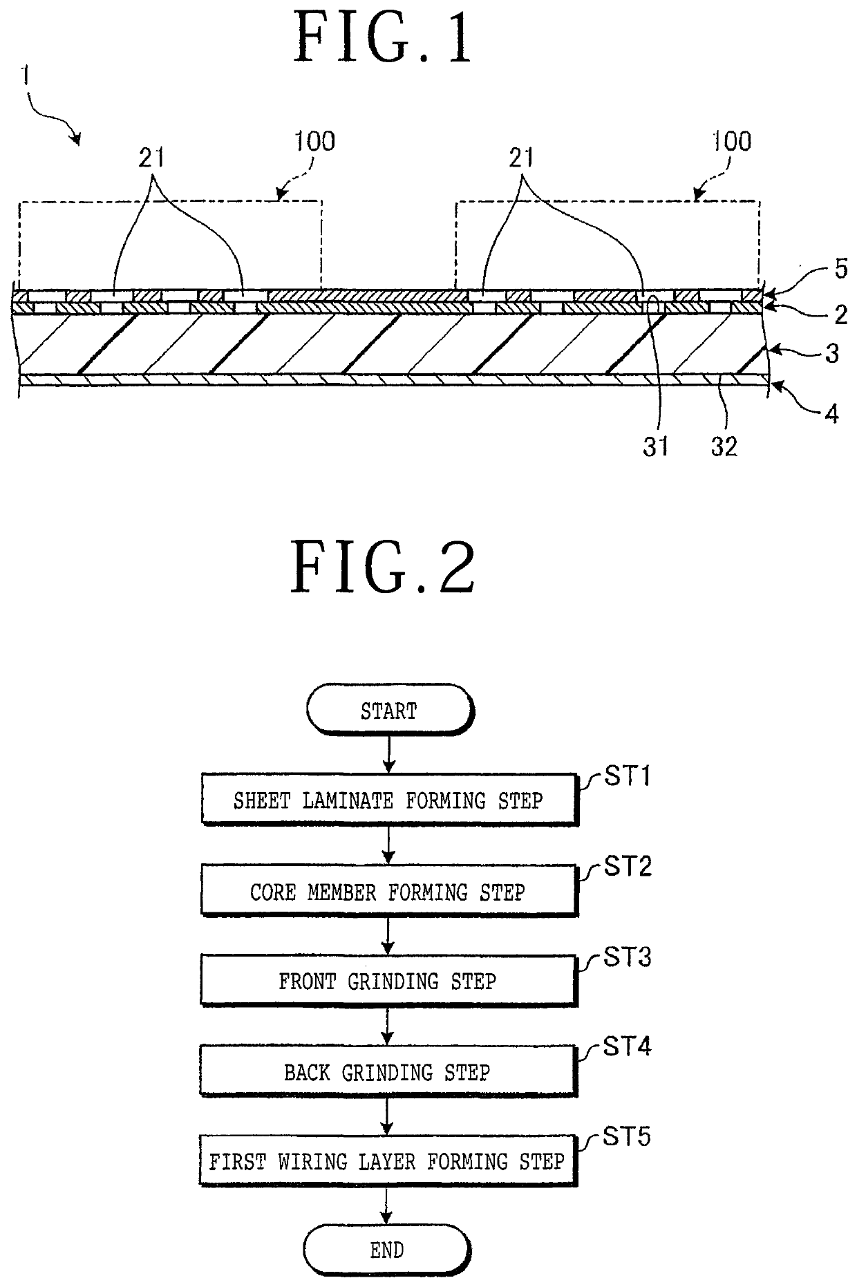
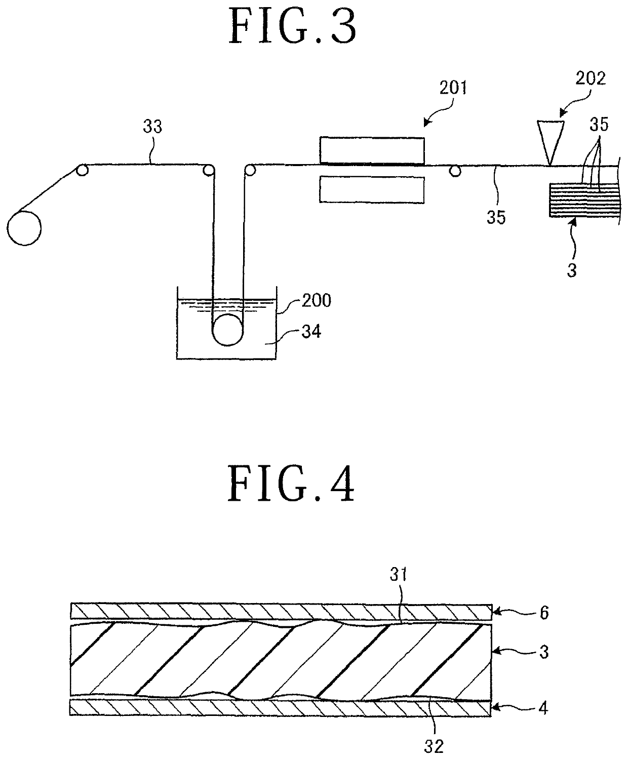
[0030]A wiring board manufacturing method according to a first preferred embodiment of the present invention will now be described with reference to the drawings. FIG. 1 is a sectional view depicting a part of a wiring board 1 to be manufactured by the wiring board manufacturing method according to the first preferred embodiment.
[0031]The wiring board 1 depicted in FIG. 1 is a wiring board on which a plurality of package device chips 100 are adapted to be mounted and connected through electrodes. More specifically, the wiring board 1 has a wiring layer 2 on the front side, and the wiring layer 2 has a plurality of electrodes 21. Each package device chip 100 has a plurality of electrodes (not depicted), which are adapted to be connected to the electrodes 21 of the wiring layer 2 of the wiring board 1. As depicted in FIG. 1, the wiring board 1 includes an insulating sheet laminate 3 having a first surface 31 and a second surface 32, a conductive wiring layer 2 formed on the first surf...
second preferred embodiment
[0054]A wiring board manufacturing method according to a second preferred embodiment of the present invention will now be described with reference to the drawings. FIG. 13 is a flowchart depicting the flow of the wiring board manufacturing method according to the second preferred embodiment. FIG. 14 is a schematic sectional view of a wiring board obtained by performing a second wiring layer forming step in the wiring board manufacturing method depicted in FIG. 13. In FIGS. 13 and 14, the same parts as those in the first preferred embodiment are denoted by the same reference numerals and the description thereof will be omitted.
[0055]The wiring board manufacturing method according to the second preferred embodiment is the same as that according to the first preferred embodiment except that a second wiring layer forming step ST6 is performed after performing the first wiring layer forming step ST5. The second wiring layer forming step ST6 is a step of forming another wiring layer 2 on ...
first modification
[0057]A wiring board manufacturing method according to a first modification of the above preferred embodiments will now be described with reference to FIG. 15. FIG. 15 is a schematic sectional view of the core member 7 after the front grinding step ST3 in the wiring board manufacturing method according to the first modification. In FIG. 15, the same parts as those in the above preferred embodiments are denoted by the same reference numerals and the description thereof will be omitted.
[0058]The wiring board manufacturing method according to the first modification is the same as that according to the above preferred embodiments except that the front grinding step ST3 is different. In the first modification, the release plate 6 is formed from a resin film such as ABF or a copper plate for forming electrodes.
[0059]In the front grinding step ST3 in the wiring board manufacturing method according to the first modification, the release plate 6 is partially removed by grinding to thereby ma...
PUM
| Property | Measurement | Unit |
|---|---|---|
| thickness | aaaaa | aaaaa |
| pressure | aaaaa | aaaaa |
| distance | aaaaa | aaaaa |
Abstract
Description
Claims
Application Information


