Connector terminal and electric connector

a technology of connecting terminals and connectors, which is applied in the direction of coupling devices, coupling contact members, two-part coupling devices, etc., can solve the problems of poor connection, difficult matching of impedances, and inability to meet impedances, so as to facilitate impedance matching, prevent poor connection, and increase the impedance

Active Publication Date: 2015-05-05
IRISO ELECTRONICS CO LTD
View PDF31 Cites 14 Cited by
  • Summary
  • Abstract
  • Description
  • Claims
  • Application Information

AI Technical Summary

Benefits of technology

[0008]The present invention is carried out to solve the aforementioned problems. That is, it is an object of the present invention to provide a connector terminal and an electric connector that make it possible to suppress poor connection, caused by foreign material adhered to a terminal surface of a mating connector, by wiping off the foreign material, and that allow impedance matching to be achieved in the connector terminal.
[0009]To this end, according to a first aspect of the present invention, there is provided a connector terminal including a circuit-board connection portion that is connected to a circuit board, a terminal portion that contacts a terminal surface of a mating connector, and a base end portion that supports an end of the terminal portion, wherein the terminal portion includes a front terminal and a rear terminal. The front terminal includes a front contact-point portion that wipes off foreign material that is adhered to the terminal surface of the mating connector. The rear terminal includes a rear contact-point portion that contacts the terminal surface of the mating connector that has been wiped by the front contact-point portion. A high-impedance portion is provided between the circuit-board connection portion and the base end portion, the high-impedance portion eliminating impedance mismatching at a terminal transmission path by canceling a reduction in an impedance at least the terminal portion as regards a transmission signal that flows from the circuit-board connection portion at a primary side to the terminal portion at a secondary side.

Problems solved by technology

When foreign material, such as substrate scrap and dust, adhered to connector terminals are interposed between the connector terminals when connecting the connector terminals to each other, poor connection occurs.
Consequently, the impedance of the terminal portions is considerably smaller than those of other portions of a connector terminal, as a result of which it becomes difficult to match the impedances.
Such a connector terminal is not desirable for, in particular, high-speed transmission of high-frequency signals.
For example, it is difficult to meet, for example, high-definition multimedia interface (trade name) standards.

Method used


Image

  • Connector terminal and electric connector
  • Connector terminal and electric connector
  • Connector terminal and electric connector

Examples


first embodiment (

FIGS. 1 to 7)

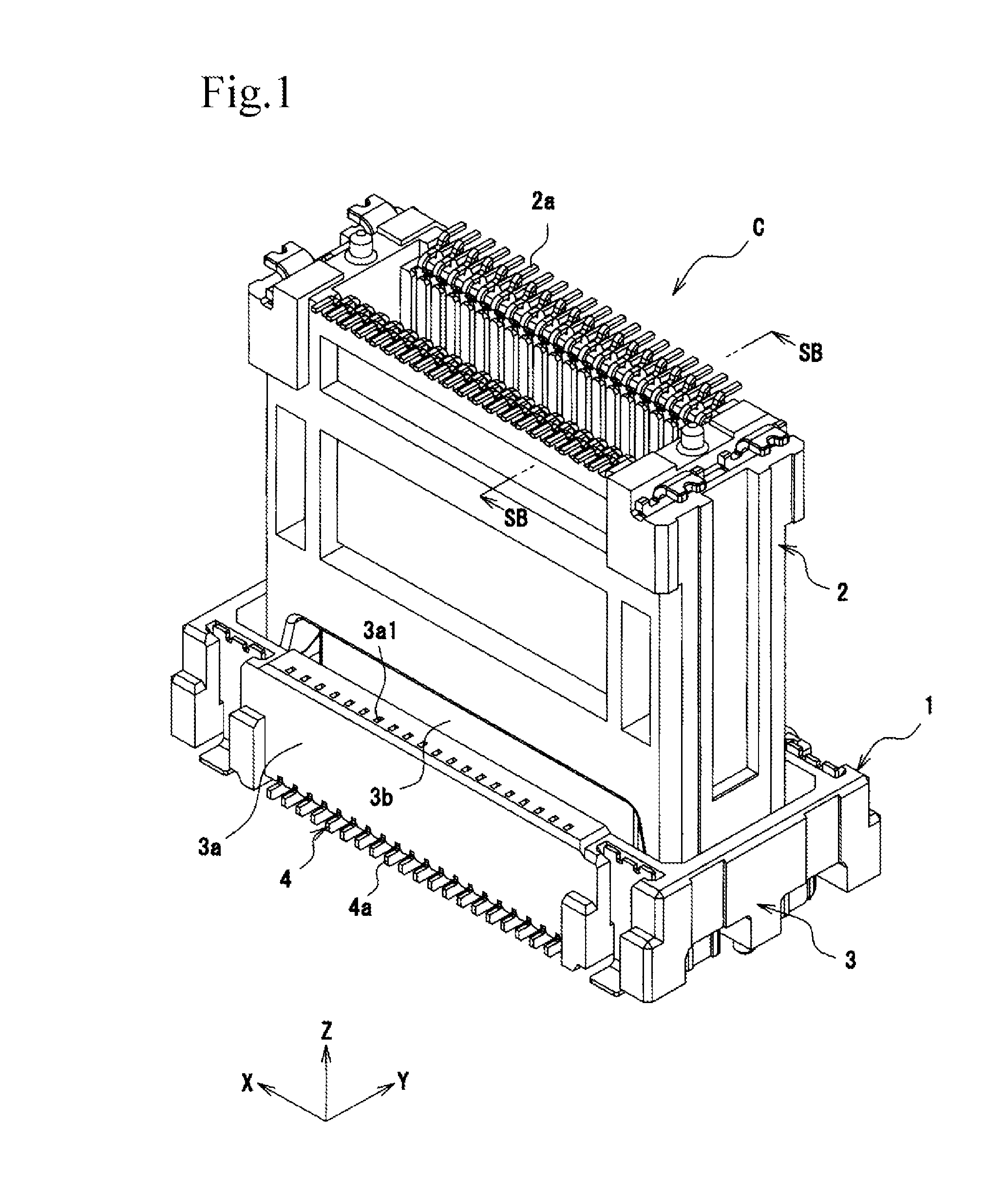
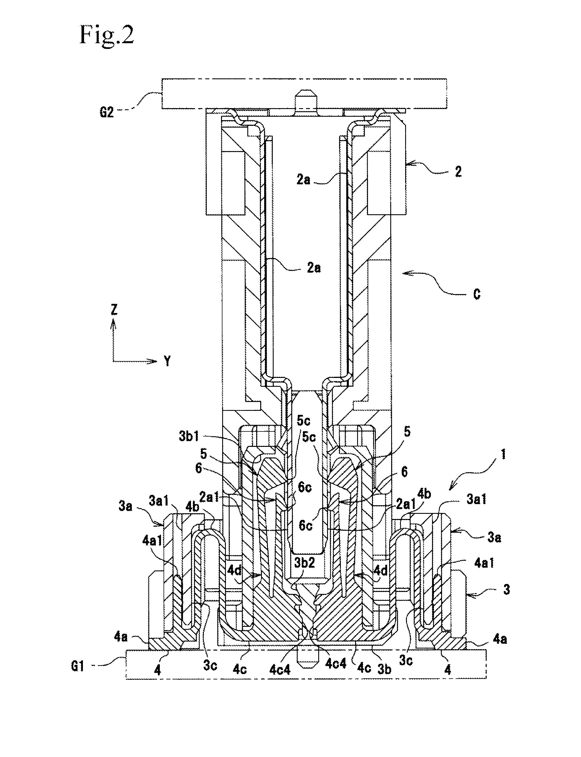
[0049]An electric connector C of the first embodiment according to the present invention includes a socket 1 and a plug 2. As shown in FIG. 2, the socket 1 is secured to a circuit board G1. As shown in FIG. 1, by fitting the socket 1 to the plug 2 (serving as a “mating connector”), the circuit board G1 and a circuit board G2 to which the plug 2 is secured are conductively connected with each other.

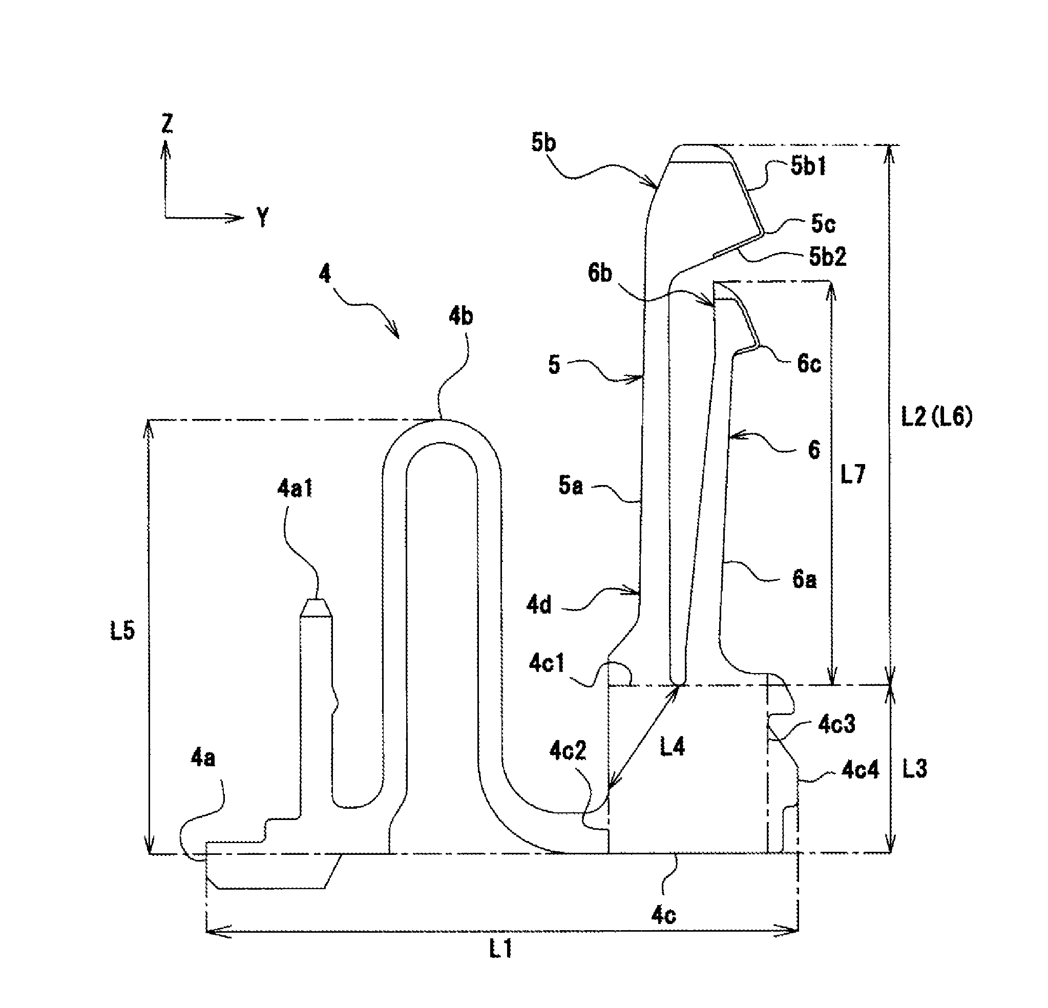
[0050]As shown in FIGS. 1 and 2, the socket 1 includes a substantially rectangular parallelepiped socket housing 3 and socket terminals 4 that are conductively connected with plug terminals 2a.

Socket Housing

[0051]The socket housing 3 is formed of insulating resin. As shown in FIGS. 1 and 2, the socket housing 3 includes a stationary housing 3a and a movable housing 3b that is displaceable relative to the stationary housing 3a by the socket terminals 4. The stationary housing 3a is provided with stationary holes 3a1 to which the socket terminals 4 are secured. The movable hous...

second embodiment (

FIGS. 8 to 10)

[0073]In the first embodiment, each socket terminal 4 is one in which the plate surface of its corresponding base end portion 4c has a substantially square shape. However, as shown in FIG. 8, each socket terminal 8 may be one in which a plate surface of a base end portion 7 has a substantially rectangular shape that is long along a short-side direction of a socket 1. FIG. 9 shows a socket terminal 8, with a length L1 in a width direction being on the order of 5 mm, a height L2 of a terminal portion 4d being on the order of 5 mm, a height L3 of a base end portion 7 being approximately 0.6 mm, and a distance L4 between the base end portion 7 and the terminal portion 4d being approximately 0.87 mm. FIG. 10 is a graph of a waveform of impedance measured at the socket terminal 8. According to FIG. 10, the waveform has a linear form whose difference between impedances is less than that of the waveform of the impedance measured at the socket terminal 4. Therefore, by bringing...

third embodiment (fig.11)

Third Embodiment (FIG. 11)

[0077]In the first and second embodiments, the socket terminals 4 and 8 including smooth, flat base end portions 4c and 7, respectively, are provided. In contrast, as shown in FIG. 11, it is possible to provide a socket terminal 12 having a through hole 11 that extends through a base end portion 4c along a plate thickness. By using such a socket terminal 12, the surface area of the base end portion 4c becomes small, so that a capacitor component is reduced. Therefore, it is possible to increase the impedances of portions beyond the base end portion 4c.

[0078]In the socket terminal 12, it is necessary to change the height of the base end portion 4c in accordance with a gap between a circuit board G2 and a circuit board G1 on which the socket terminal 12 is mounted. The larger the height of the base end portion 4c, the larger the capacitor component of a movable portion 4b. Since this causes a distance L4 between the movable portion 4b and a terminal portion ...


PUM


Abstract

A socket terminal includes front and rear terminals. The front terminal includes a front contact-point portion that wipes off foreign material adhered to a terminal surface of a plug terminal. The rear terminal includes a rear contact-point portion that contacts the terminal surface wiped by the front contact-point portion. The socket terminal also includes a movable portion between a circuit-board connection portion and circuit board. The movable portion cancels a reduction in impedance of at least the front terminal and rear terminal for a transmission signal flowing from the circuit-board connection portion connected to the circuit board. This can provide a socket terminal allowing the rear contact-point portion to contact the terminal surface from which foreign material has been wiped off, and allowing impedance mismatching at a terminal transmission path to be eliminated; and to provide an electric connector including the socket terminal.

Description

BACKGROUND OF THE INVENTION[0001]1. Field of the Invention[0002]The present invention relates to a connector terminal and an electric connector that are capable of wiping off foreign material and that are suitable for high-speed transmission.[0003]2. Description of the Related Art[0004]Development in information processing technology and communication technology has dramatically increased the amount of data that is handled by on-vehicle equipment and consumer electric devices. High-speed transmission technology, such as differential transmission (balanced transmission), that can achieve effective transmission of a large amount of data in a short time is used in various electric devices. Therefore, as regards connectors that form part of a transmission path, those that allow impedance matching and that are suitable for high-speed transmission that does not cause distortion in a signal waveform are used.[0005]The basic structure of a connector terminal therefor includes a circuit-boar...

Claims


Application Information

Patent Timeline
Patent Type & Authority Patents(United States)
IPC IPC(8): H01R24/00H01R12/70H01R13/193H01R13/52H01R13/6474
CPCH01R13/6474H01R12/70H01R13/52H01R13/193H01R12/716H01R13/26H01R12/91H01R13/2457
Inventor TAKAKI, MASATO
Owner IRISO ELECTRONICS CO LTD
Why Eureka
Try Eureka