TFT substrate and light emitting display device including the same

a thin film transistor and display device technology, applied in the field of thin film transistors and light-emitting display devices, can solve the problems of insufficient length of driving tft channels, inevitably decreasing the size of pixels, etc., and achieve the effect of stable driving properties

Active Publication Date: 2022-02-08
LG DISPLAY CO LTD
View PDF2 Cites 3 Cited by
  • Summary
  • Abstract
  • Description
  • Claims
  • Application Information

AI Technical Summary

Benefits of technology

[0008]An advantage of the present disclosure is to provide a TFT substrate and a light emitting display device including the same which can secure a length of a channel of a driving TFT using polycrystalline silicon and achieve a stable driving property.

Problems solved by technology

However, as a resolution of a display device increases, a size of a pixel inevitably decreases.
Accordingly, there is a problem that a driving TFT does not have a channel with a long enough length of as required.

Method used


Image

  • TFT substrate and light emitting display device including the same
  • TFT substrate and light emitting display device including the same
  • TFT substrate and light emitting display device including the same

Examples


Embodiment Construction

[0024]Reference will now be made in detail to exemplary aspects, examples of which are illustrated in the accompanying drawings. The same reference numbers may be used throughout the drawings to refer to the same or like parts.

[0025]A TFT substrate of aspects of the present disclosure may be applied to all sorts of electronic devices using a TFT. For example, a TFT substrate may be applied to various electronic devices including a display device, a sensor panel, and the like.

[0026]For the purpose of explanations, aspects of the present disclosure are described with a TFT substrate used for an organic light emitting display device (OLED) by way of example.

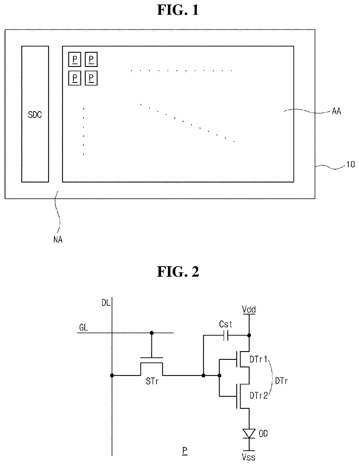
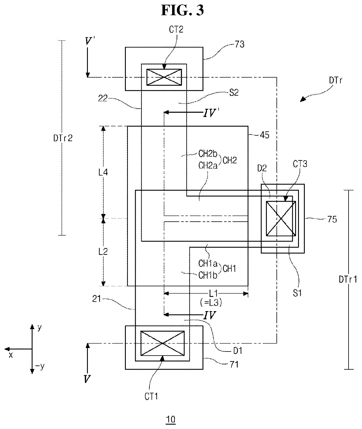
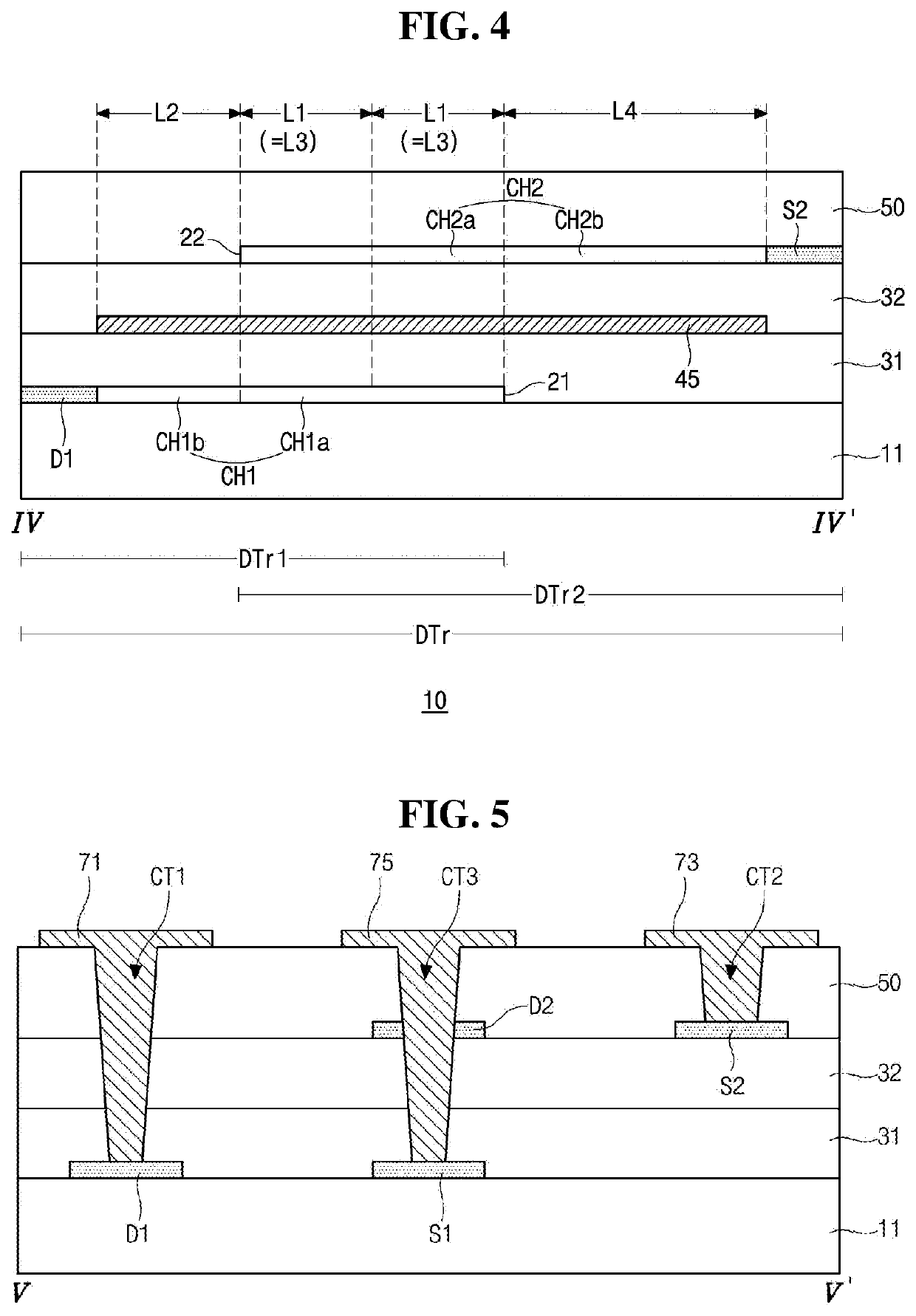
[0027]FIG. 1 is a plan view schematically illustrating a TFT substrate of an OLED display device according to the present disclosure. FIG. 2 is a circuit diagram schematically illustrating a pixel region of FIG. 1.

[0028]Referring to FIGS. 1 and 2, the TFT 10 may include a display region AA as an active region for displaying an image...


PUM

PropertyMeasurementUnit
lengthaaaaaaaaaa
channel lengthaaaaaaaaaa
channel lengthsaaaaaaaaaa

Abstract

A thin film transistor (TFT) substrate comprises a TFT located on a substrate and including a gate electrode, a first semiconductor layer and a second semiconductor layer, wherein the first semiconductor layer, the gate electrode and the second semiconductor layer vertically stacked, and the first and second semiconductor layers are made of polycrystalline silicon, and wherein the first and second semiconductor layers are electrically connected to each other in series and respectively include first and second channel portions, and at least one of the first and second channel portions has a bent structure in a plan view.

Description

CROSS REFERENCE TO RELATED APPLICATION[0001]The present application claims the priority benefit of Korean Patent Application No. 10-2018-0109344 filed in Republic of Korea on Sep. 13, 2018, which is hereby incorporated by reference in its entirety.BACKGROUNDField of the Disclosure[0002]The present disclosure relates to a display device, and more particularly, to a thin film transistor (TFT) substrate and a light emitting display device including the same. Although the present disclosure is suitable for a wide scope of applications, it is particularly suitable for providing a TFT substrate and a light emitting display device including the same which can secure a length of a channel of a driving TFT using polycrystalline silicon and achieve a stable driving characteristic.Description of the Background[0003]Generally, a thin film transistor (TFT) substrate in which TFTs are formed is used for a light emitting display device, including an organic light emitting display device (OLED) as ...

Claims


Application Information

Patent Timeline
Patent Type & Authority Patents(United States)
IPC IPC(8): H01L29/786H01L29/417H01L27/32H01L29/423H01L27/12
CPCH01L29/78696H01L29/41733H01L29/42384H01L29/78618H01L29/78621H01L29/78672H01L27/1251H01L27/1255H01L29/78633H10K59/00H10K59/12H01L27/1222H01L29/786H01L27/1214H10K59/1213H10K50/00
Inventor OH, KUM-MI
Owner LG DISPLAY CO LTD
Why Eureka
Try Eureka