Supercharge Your Innovation With Domain-Expert AI Agents!

Semiconductor device including dummy gate patterns and manufacturing method thereof

a technology of semiconductor devices and dummy patterns, applied in semiconductor devices, electrical devices, transistors, etc., can solve problems such as undercutting of dummy patterns

Active Publication Date: 2022-03-01
SAMSUNG ELECTRONICS CO LTD
View PDF8 Cites 0 Cited by
  • Summary
  • Abstract
  • Description
  • Claims
  • Application Information

AI Technical Summary

Benefits of technology

The proposed design and manufacturing method result in stable dummy patterns that prevent leaning phenomena and enhance pattern density and patternability, reducing defects in subsequent semiconductor device processes.

Problems solved by technology

However, undercuts may occur in the dummy patterns, or the dummy patterns may be formed in an asymmetrical shape.
Such unstable dummy patterns may act as a defect source in subsequent processes.

Method used


Image

  • Semiconductor device including dummy gate patterns and manufacturing method thereof
  • Semiconductor device including dummy gate patterns and manufacturing method thereof
  • Semiconductor device including dummy gate patterns and manufacturing method thereof

Examples


Embodiment Construction

[0030]Hereinafter, example embodiments of the inventive concept will be described in detail with reference to the accompanying drawings to clearly explain the technical idea of the inventive concept.

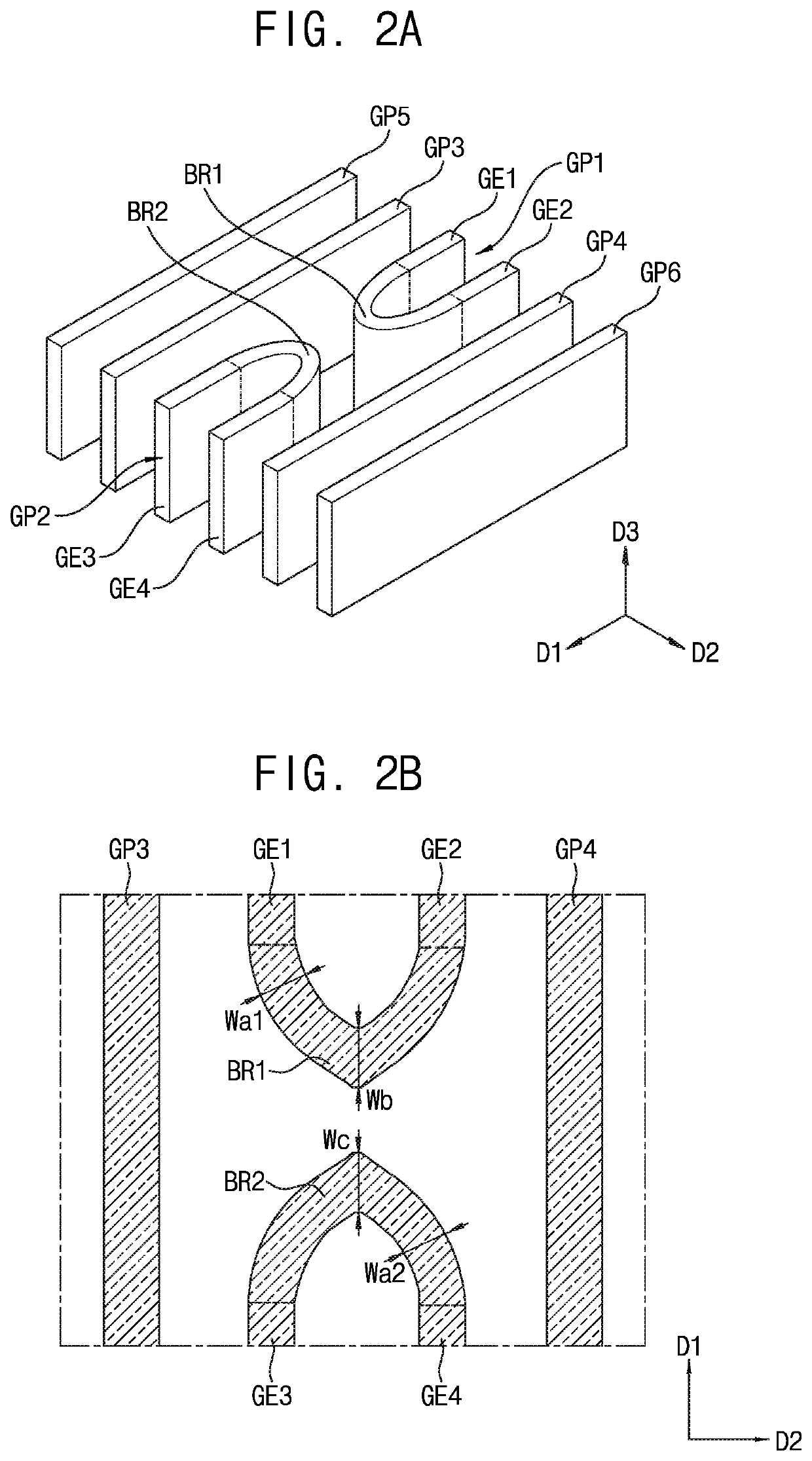
[0031]FIG. 1A is a perspective view for describing a semiconductor device according to an example embodiment of the present inventive concept. FIG. 1B is a plan view of a partial region of FIG. 1A.

[0032]Referring to FIGS. 1A and 1B, the semiconductor device according to the example embodiment of the present inventive concept may include a plurality of gate patterns GP1, GP2, GP3, and GP4 on a substrate. The gate patterns GP1, GP2, GP3, and GP4 may include a first gate pattern GP1 and a second gate pattern GP2. The gate patterns GP1, GP2, GP3, and GP4 may include a conductive material. However, the present inventive concept is not limited thereto, and the gate patterns GP1, GP2, GP3, and GP4 may be made of a non-metal material such as polysilicon. Further, the gate patterns GP1, GP2, GP3,...


PUM

PropertyMeasurementUnit
U-shapeaaaaaaaaaa
widthaaaaaaaaaa
pattern densityaaaaaaaaaa

Abstract

A semiconductor device may include: a dummy gate structure including a first gate pattern in which dummy gate lines extending in one direction are connected to each other on a substrate, and a second gate pattern in which dummy gate lines extending in the one direction are connected to each other on the same line with the first gate pattern; and a third gate pattern extending in parallel with the dummy gate structure on one side of the dummy gate structure.

Description

CROSS-REFERENCE TO THE RELATED APPLICATION[0001]This U.S. non-provisional patent application claims priority under 35 U.S.C. § 119 to and the benefit of Korean Patent Application No. 10-2019-0047578, filed on Apr. 23, 2019, in the Korean Intellectual Property Office (KIPO), the disclosure of which is incorporated herein by reference in its entirety.BACKGROUND1. Field[0002]The present inventive concept relates to a semiconductor device including gate patterns and a manufacturing method thereof.2. Description of Related Art[0003]Dummy patterns may be formed in a partial region of a substrate to increase pattern density and patternability. However, undercuts may occur in the dummy patterns, or the dummy patterns may be formed in an asymmetrical shape. Such unstable dummy patterns may act as a defect source in subsequent processes.SUMMARY[0004]The present inventive concept is directed to providing a semiconductor device including a stable dummy pattern.[0005]In addition, the present inv...

Claims


Application Information

Patent Timeline
Patent Type & Authority Patents(United States)
IPC IPC(8): H01L29/66H01L21/8234H01L29/78H01L27/088
CPCH01L29/66545H01L21/823431H01L27/0886H01L29/66795H01L29/785H01L27/0207H01L29/7831H01L29/4236H01L21/823462H01L21/82345
Inventor KIM, DONGHYUNSONG, INHYUNJEON, YEONGMINPARK, SEJINPARK, JUYUNBAEK, JONGHOONSHIN, TAEYEONJEONG, SOOYEON
Owner SAMSUNG ELECTRONICS CO LTD
Features
  • R&D
  • Intellectual Property
  • Life Sciences
  • Materials
  • Tech Scout
  • Unparalleled Data Quality
  • Higher Quality Content
  • 60% Fewer Hallucinations
Learn More