Testing of LED devices during pick and place operations

a technology of led devices and pick-and-place operations, which is applied in the direction of semiconductor devices, semiconductor/solid-state device testing/measurement, electrical apparatus, etc., can solve the problems of slow apparatus for such testing, less compact, complex, etc., and achieves improved speed of apparatus, reduced complexity of apparatus, and compact apparatus

Active Publication Date: 2022-03-15
ASMPT SINGAPORE PTE LTD
View PDF12 Cites 0 Cited by
  • Summary
  • Abstract
  • Description
  • Claims
  • Application Information

AI Technical Summary

Benefits of technology

[0006]Accordingly, a pick and place apparatus is provided. The apparatus may be for LED testing. The apparatus may comprise a test station or testbed which may power or activate a group of LEDs. The group of LEDs may comprise a plurality of LEDs. The apparatus may comprise a bond head which may pick the group of LEDs from a wafer and place that group of LEDs onto the test station to be tested. The apparatus may comprise an optical sensor which measures the optical characteristics of the group of LEDs on the test station. The bond head may be configured to provide an optical path which allows light from the LEDs to pass through the bond head to the optical sensor. In this way, the optical sensor can be located on the same side of the LEDs as the bond head, which reduces the complexity of the apparatus and provides for a more compact apparatus. Also, by testing groups of LEDs, the speed of the apparatus is improved.
[0007]The portion of the bond head may be translucent. That is to say, the portion of the bond head may allow for transmission of light therethrough.
[0035]The translucent holder may be elastic and may provide for contact adhesion between said translucent holder and at least one LED from said group of LEDs.

Problems solved by technology

However, apparatus for performing such testing can be slow, complex and less compact than is desirable.

Method used


Image

  • Testing of LED devices during pick and place operations
  • Testing of LED devices during pick and place operations
  • Testing of LED devices during pick and place operations

Examples


Embodiment Construction

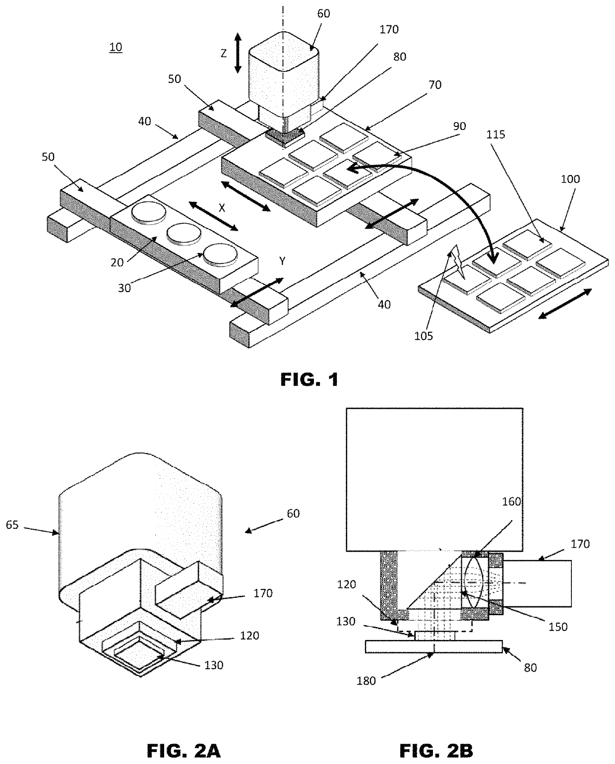
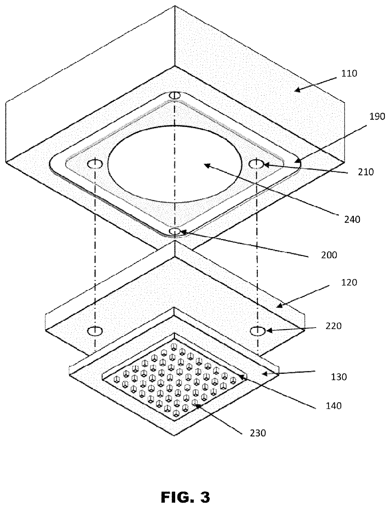
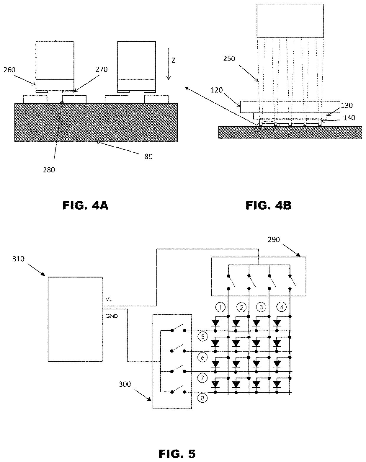
[0067]Before discussing the embodiments in any more detail, first an overview will be provided. Some embodiments provide a pick and place LED testing apparatus which has a bond head configured to allow light from a group of LEDs to pass at least partially through it during testing. This enables groups of LEDs to be picked from a source wafer, placed on a test board for optical, and optionally electrical, testing. The optical, and optionally electrical, characteristics of that group of LEDs are determined and the LEDs are then placed on one of a plurality of different bin carriers depending on an average optical, and optionally electrical, characteristic of that group of LEDs. This means that each of the different bin carriers fills with groups of LEDs having similar optical characteristics. An example of an optical characteristic is a colour coordinate of an LED, wherein each value in a colour coordinate represents a position of a colour in a colour space, such as different shades o...


PUM

PropertyMeasurementUnit
sizesaaaaaaaaaa
optical characteristicaaaaaaaaaa
translucentaaaaaaaaaa

Abstract

A pick and place LED testing apparatus, comprising: a test station operative in use to power a group of LEDs; a bondhead operative in use to pick said group of LEDs from a source wafer and place said group of LEDs on said test station for testing; and an optical sensor operative in use to measure an optical characteristic of said group of LEDs when tested, wherein at least a portion of said bondhead is translucent to provide an optical path from said group of LEDs to said optical sensor.

Description

FIELD OF THE INVENTION[0001]The invention relates to an apparatus and method for testing light emitting diode (LED) devices during pick and place operations.BACKGROUND[0002]Techniques for testing LEDs exist. Such techniques typically pick an LED and then place it against an electrical circuit to provide electrical power to perform optical and / or electrical characteristic testing in order to verify the characteristics and operation of that LED. However, apparatus for performing such testing can be slow, complex and less compact than is desirable.[0003]It would be beneficial to provide an arrangement which is faster, simpler and more compact as compared to the prior art.SUMMARY OF THE INVENTION[0004]It is thus an object of this invention to seek to provide an arrangement which overcomes at least some of the aforementioned problems of the prior art.[0005]According to a first aspect of the present invention, there is provided a pick and place LED testing apparatus, comprising: a test st...

Claims


Application Information

Patent Timeline
Patent Type & Authority Patents(United States)
IPC IPC(8): H01L21/66H01L33/00G01R31/26
CPCH01L22/14H01L22/22H01L22/24H01L22/30H01L33/005G01R31/2635H01L2933/0066H01L22/12
Inventor LEE, SHUN YANWONG, SAI KITYUEN, CHI WAHMAK, KA YEEWIDDOWSON, GARY PETER
Owner ASMPT SINGAPORE PTE LTD
Why Eureka
Try Eureka