

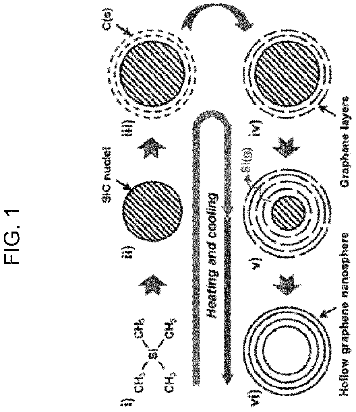
Method for producing graphene nanospheres
a graphene nanosphere and nano-sphere technology, applied in the field of graphene nanosphere manufacturing, can solve the problem that the template used by the particles must be removed, and achieve the effect of superior mechanical and electrical properties of graphen
- Summary
- Abstract
- Description
- Claims
- Application Information
AI Technical Summary
Benefits of technology
Problems solved by technology
Method used
Image

Examples
example 1
[0051]Hydrogen gas and tetramethylsilane (TMS) were placed at a flow rate ratio of H2 / TMS of 320 in a reactor, heated under a pressure of 550 torr, reacted for 1 hr at a maximum temperature of 2100° C., and then cooled to room temperature.
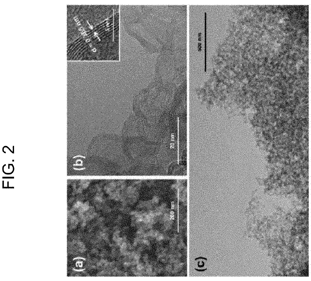
[0052]FIG. 2 shows (a) a scanning electron microscope (SEM) image and (b) and (c) transmission electron microscope (TEM) images of the hollow graphene nanospheres manufactured in Example 1 of the present invention. With reference to FIG. 2, it can be seen that the hollow graphene nanospheres had a spherical shape ((a)) and that the spherical graphene nanospheres were hollow ((b), (c)). As is apparent from the high-resolution transmission electron microscope (HRTEM) image in (b) of FIG. 2, graphene had a layered structure. With reference to FIG. 2, it can be confirmed that the hollow graphene nanospheres had an inner diameter of 20 to 30 nm.
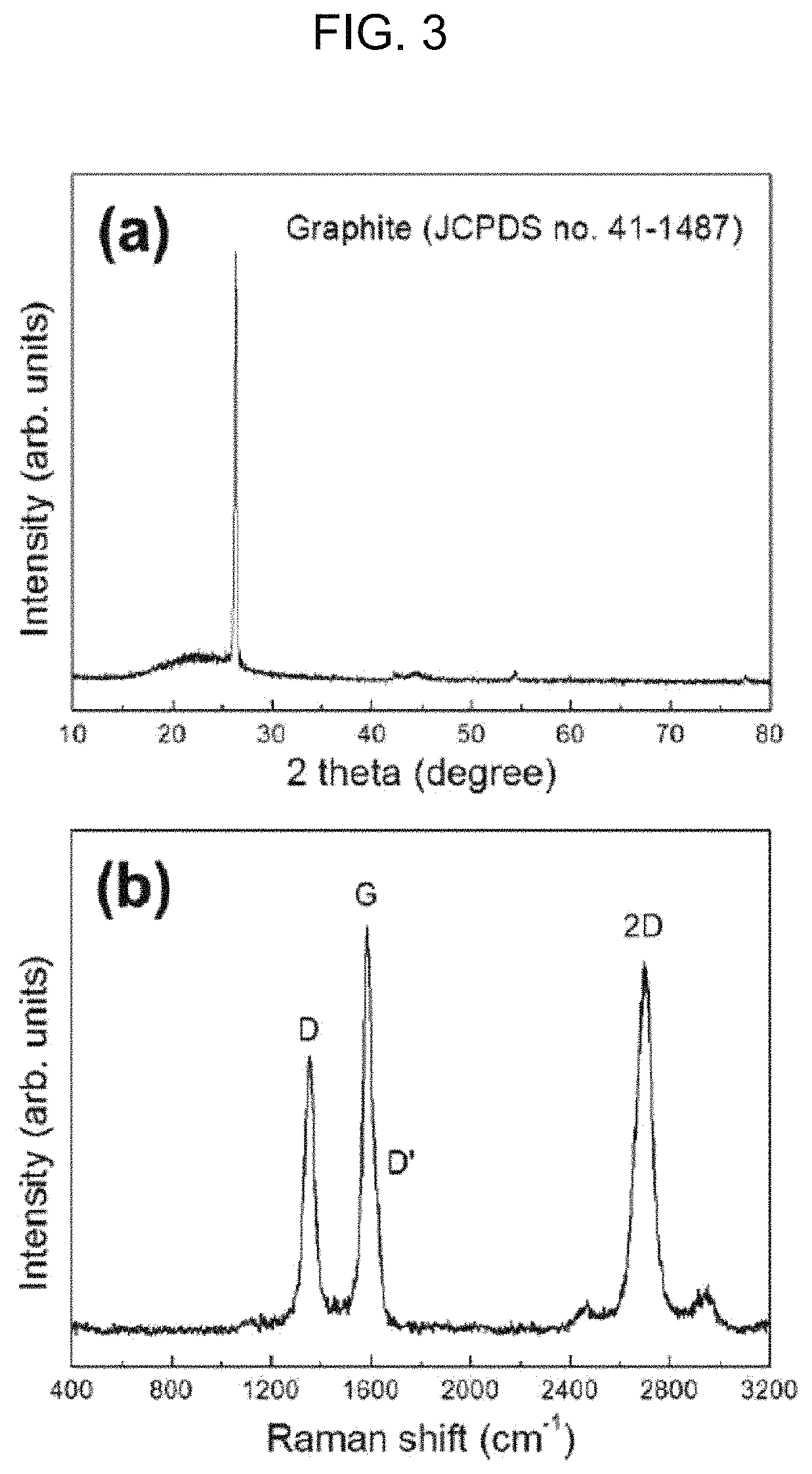
[0053]FIG. 3 shows (a) an XRD graph and (b) a Raman spectrum of the hollow graphene nanospheres manufactured i...
example 2
[0055]The present example was performed in the same manner as in Example 1, with the exception that the maximum temperature was set to 1500° C.
[0056]FIG. 4 shows (a) a TEM image and the results of energy-dispersive spectroscopy (EDS) and (b) a Raman spectrum of the graphene nanospheres manufactured in Example 2 of the present invention. With reference to FIG. 4, in the graphene nanospheres produced at a low temperature of 1500° C., particles in which the insides of the graphene nanospheres were filled with silicon carbide (SiC) nanocrystal were observed, unlike the hollow graphene nanospheres of Example 1 manufactured at 2100° C.
[0057]In Example 2, 60% of the reaction product was hollow graphene nanospheres, and the remaining 40% was graphene nanospheres, the insides of which were filled.
example 3
[0058]The present example was performed in the same manner as in Example 1, with the exception that the maximum temperature was set to 1900° C.
[0059]FIG. 5 shows (a) a SEM image, (b) an EDS spectrum and (c) a TEM image of the graphene nanospheres manufactured in Example 3 of the present invention. With reference to FIG. 5, in the graphene nanospheres produced at a temperature of 1900° C., the number of hollow graphene nanospheres was significantly increased, unlike the graphene nanospheres of Example 2 manufactured at 1500° C. As shown in FIG. 5, the inner diameter of the hollow graphene nanospheres was 20 to 30 nm.
[0060]In Example 3, 80% of the reaction product was hollow graphene nanospheres, and the remaining 20% was graphene nanospheres, the insides of which were filled.
PUM
| Property | Measurement | Unit |
|---|---|---|
| pressure | aaaaa | aaaaa |
| temperature | aaaaa | aaaaa |
| temperature | aaaaa | aaaaa |
Abstract
Description
Claims
Application Information