Process for forming cone shaped solder for chip interconnection

a technology of cone-shaped solder and interconnection, which is applied in the direction of sustainable manufacturing/processing, semiconductor/solid-state device details, final product manufacturing, etc., can solve the problems of significant deviation from planarity, non-planarity across the chip site, and inability to tolera

Inactive Publication Date: 2001-08-23
INT BUSINESS MASCH CORP
View PDF0 Cites 17 Cited by
  • Summary
  • Abstract
  • Description
  • Claims
  • Application Information

AI Technical Summary

Benefits of technology

[0021] The present invention relates to, in a second aspect, a process for forming non-spherical shapes in solder interconnects comprising the steps of: (a) providing a semiconductor wafer and a substrate for mounting the wafer; (b) applying a masking layer to the wafer or to the substrate; (c) patterning and developing a plurality of openings in the masking layer; (d) forming a plurality of solder interconnects by plating a layer of solder into the plurality of openings in the masking layer; and (e) molding the plurality of solder interconnects into a non-spherical shape, wherein the non-spherical shape of the plurality of solder interconnects facilitates joining of the wafer and the substrate in a non-planar environment.
[0037] Preferably, step (h) comprises molding the solder to form a cone shaped wherein the cone shape has a taper about 15 to 25 degrees from the vertical. More preferably, step (h) comprises molding the solder with a coining die to form the cone shaped solder. The coining die may comprise a rigid, non-solder wettable plate having an array of conically shaped cavities. Preferably, step (h) comprises molding the solder with a heated coining die comprising a rigid, non-solder wettable plate having an array of conically shaped cavities. Most preferably, step (h) comprises molding the solder with a coining die comprising a rigid, non-solder wettable plate having conically shaped cavities and trapezoidally shaped cavities. The coining die molds a portion of the solder into trapezoidal shapes as stand-offs wherein the stand-offs control the collapse of the solder during contact between a semiconductor wafer and a substrate.

Problems solved by technology

What cannot be tolerated, however, is any significant deviation from planarity between the chip surface and the substrate surface since electrical interconnection cannot occur unless the solder bump on the chip physically contacts the substrate.
Multi-layer ceramic (MLC) chip carriers with flip chip technology often possess, due to design, the tendency to have localized bulges at the location of underlying substrate vias.
In addition, residual camber (non-planarity) from sintering the substrate can lead to further non-planarity across the chip site.
Both surfaces are flat which would not overcome the non-planarity of a chip and substrate when joining such components in flip chip packaging.
The flat top surface of the solder would not overcome the non-planarity of the electronic components in an electronic module.

Method used


Image

  • Process for forming cone shaped solder for chip interconnection
  • Process for forming cone shaped solder for chip interconnection
  • Process for forming cone shaped solder for chip interconnection

Examples


Embodiment Construction

)

[0060] In describing the preferred embodiment of the present invention, reference will be made herein to FIGS. 1-9 of the drawings in which like numerals refer to like features of the invention. Features of the invention are not necessarily shown to scale in the drawings.

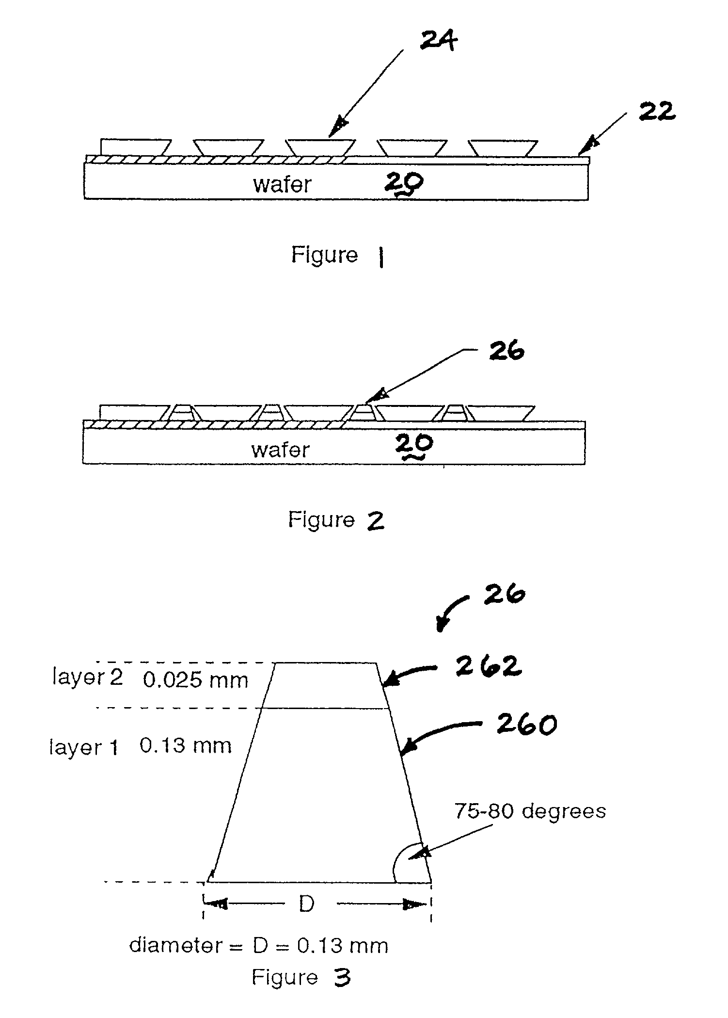
[0061] In FIG. 1, a semiconductor chip 20 has been processed through all prior processes such as device formation, and wiring layers as shown. At this stage, the wafer 20 has a deposited blanket seed layer 22 such as a chromium copper alloy or a titanium copper alloy. Upon the seed layer 22, a thick film resist 24 is deposited, patterned and developed according to a desired array for solder interconnections. A typical photoresist used in this process is Riston.TM..

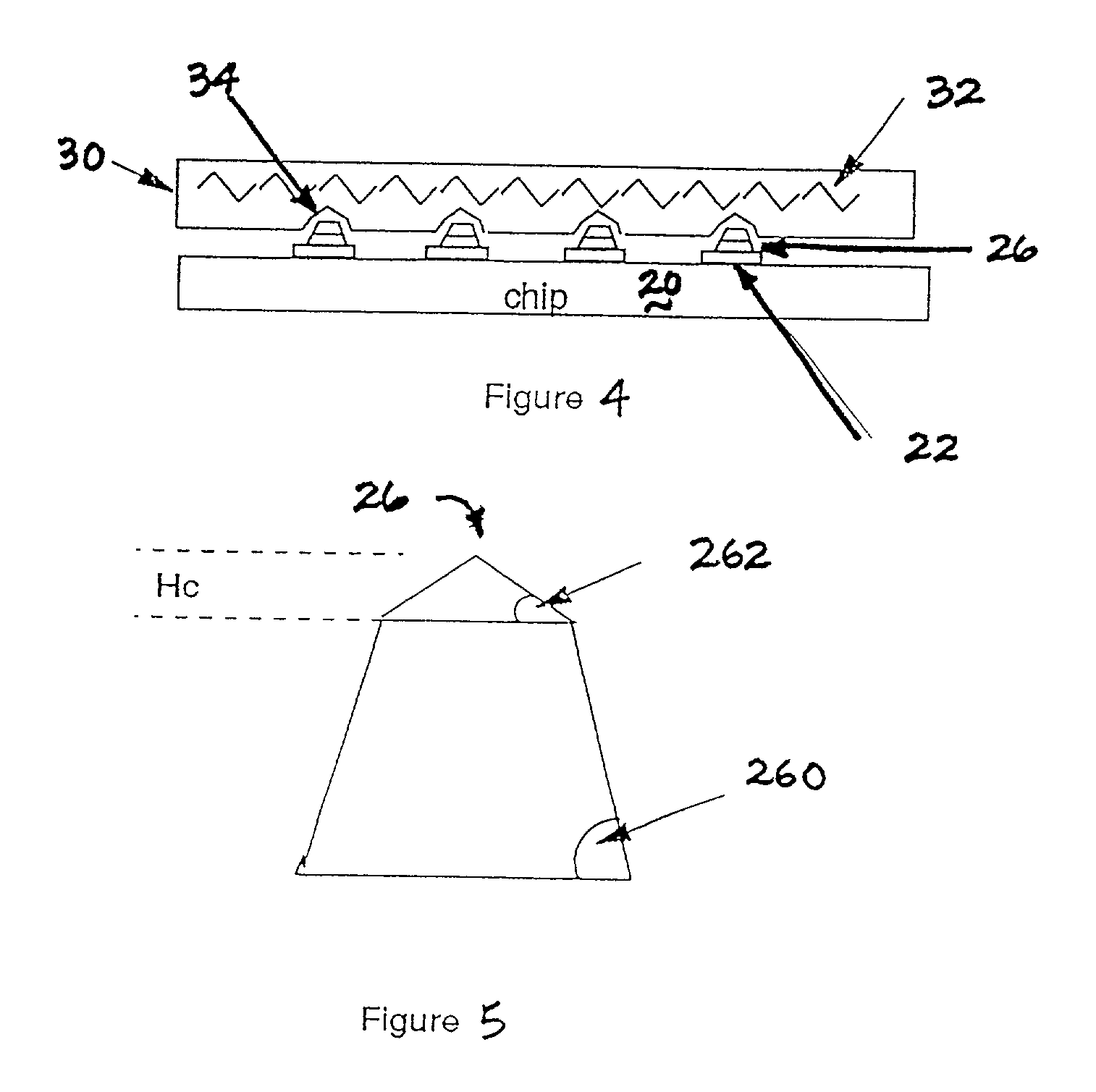
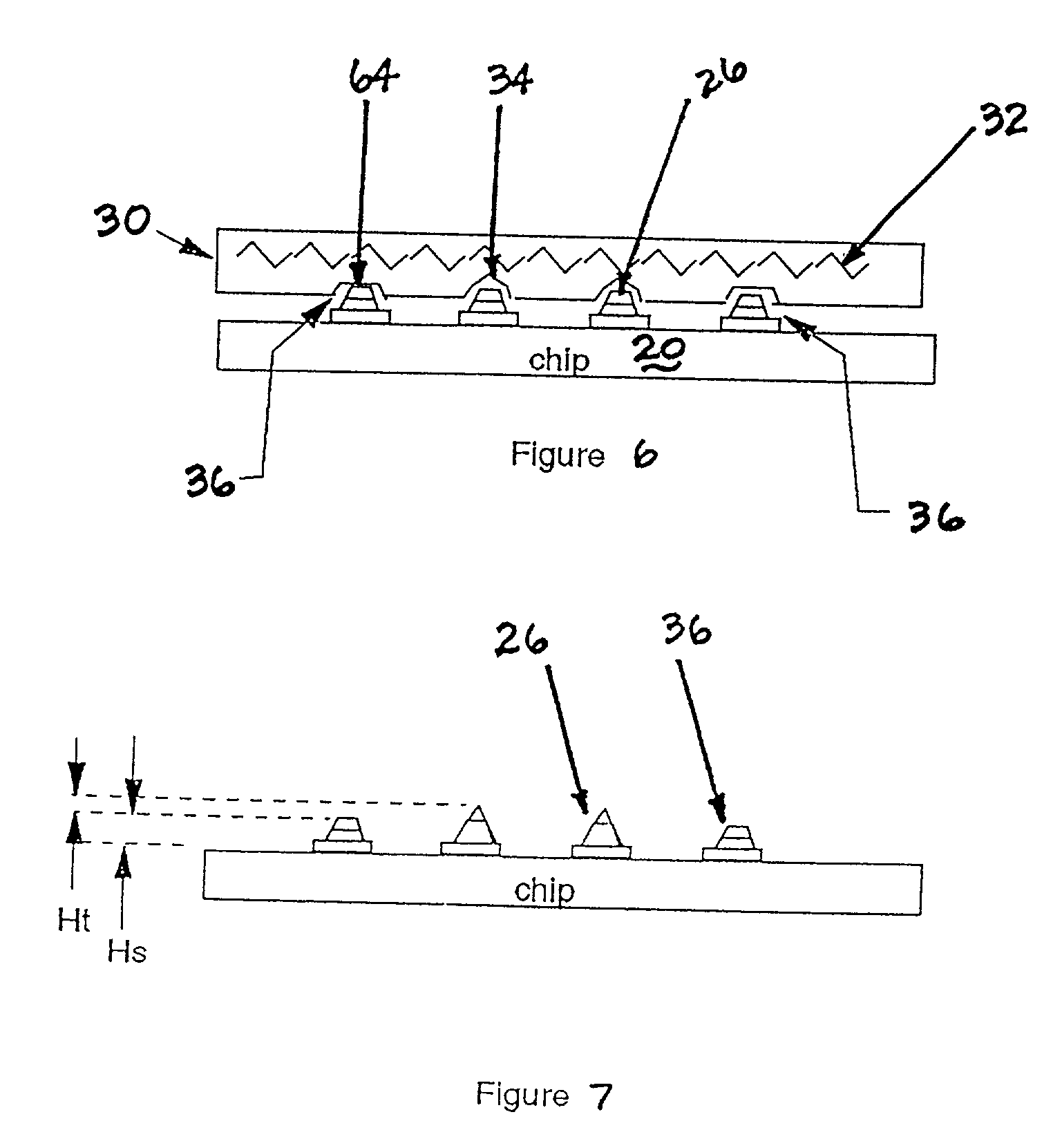
[0062] Once the photo resist 24 has been developed, a solder preform is formed in the exposed areas of the resist. Preferably, a two layer solder preform 26 is plated or otherwise deposited as shown in FIGS. 2 and 3. The first solder layer 260 may be a hi...


PUM

PropertyMeasurementUnit
diameteraaaaaaaaaa
thicknessaaaaaaaaaa
thicknessaaaaaaaaaa

Abstract

A method of forming non-spherically shaped solder interconnects, preferably conical, for attachment of electronic components in an electronic module. Preferably, the solder interconnects of the present invention are cone shaped and comprise of depositing a first solder followed by a second solder having a lower reflow temperature than the first solder. Warm placement of the electronic component at a somewhat elevated temperature than room temperature but less than the solder reflow temperature reduces the force required during placement of a semiconductor chip to a substrate. After warm placement, reflow of the module occurs at the lower reflow temperature of the second solder. The conical shape of the solder interconnects are formed by a heated coining die which may also coin a portion of the interconnects with flat surfaces for stand-offs. The ability of the cone shaped solder interconnects to meet the opposing surface of a chip or substrate at different heights accommodates the camber typically associated with chip and substrate surfaces.

Description

[0001] Aspects of the present invention are related to subject matter disclosed in co-pending applications entitled "Dielectric Interposer for Chip to Substrate Soldering," Attorney Docket No. FI9-98-129, and "Underfill Preform Interposer for Joining Chip to Substrate," Attorney Docket No. FI9-97-215 filed on even date herewith and assigned to the assignee of the present invention.[0002] 1. Field of the Invention[0003] This invention relates to the manufacture of electronic modules, namely flip chip packaging, utilizing an improved method of assembling the module. The improved method allows for enhanced contact with less stressing on the solder joints used to electrically interconnect a chip and a substrate resulting in an electronic module having higher integrity and reliability.[0004] 2. Description of Related Art[0005] Multi-layer ceramic electronic components are typically joined together by soldering pads on a surface of one of the electronic components to corresponding pads on...

Claims


Application Information

Patent Timeline
Patent Type & Authority Applications(United States)
IPC IPC(8): B23K1/00H01L21/60H01L23/48H01L23/485H05K3/24H05K3/30H05K3/34
CPCH01L24/11H01L24/81H01L2224/0401H01L2224/0603H01L2224/06505H01L2224/11002H01L2224/11472H01L2224/1184H01L2224/13099H01L2224/13111H01L2224/1403H01L2224/14505H01L2224/81136H01L2224/8121H01L2224/81815H01L2924/01004H01L2924/01013H01L2924/01022H01L2924/01027H01L2924/01029H01L2924/01042H01L2924/01049H01L2924/01074H01L2924/01078H01L2924/01082H01L2924/01322H01L2924/14H05K3/303H05K3/3436H05K3/3457H05K3/3473H05K2201/10992H05K2203/0113H05K2203/0465H01L2924/01005H01L2924/01006H01L2924/01024H01L2924/01033H01L2924/0105H01L2924/014H05K2201/2036H01L2924/10253H01L2924/00H01L2224/10135H01L2224/81139H01L24/13H01L2224/05666H01L2224/05671H01L2224/13017H01L2224/13019H01L2224/13082H01L2224/13116H01L2224/14H01L2224/14051H01L2224/141H01L2224/16058H01L2224/16238H01L2924/15787H01L2924/351Y02P70/50H01L2924/01083H01L2924/013H01L2924/00013H01L2924/00014H01L23/48
Inventor BROFMAN, PETER J.FAROOQ, SHAJIKNICKERBOCKER, JOHN U.LANGENTHAL, SCOTT I.RAY, SUDIPTA K.STALTER, KATHLEEN A.
Owner INT BUSINESS MASCH CORP
Why Eureka
Try Eureka