

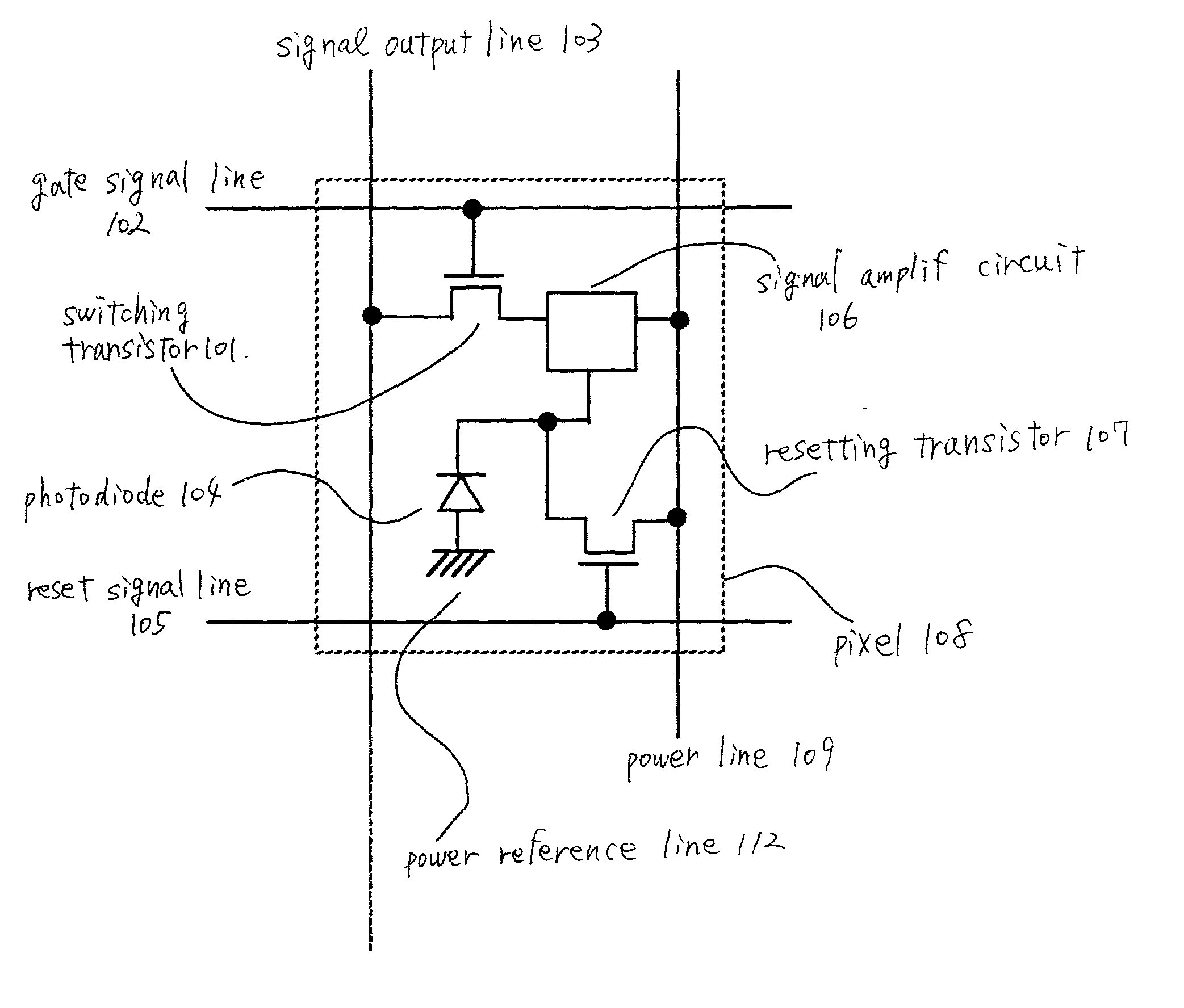
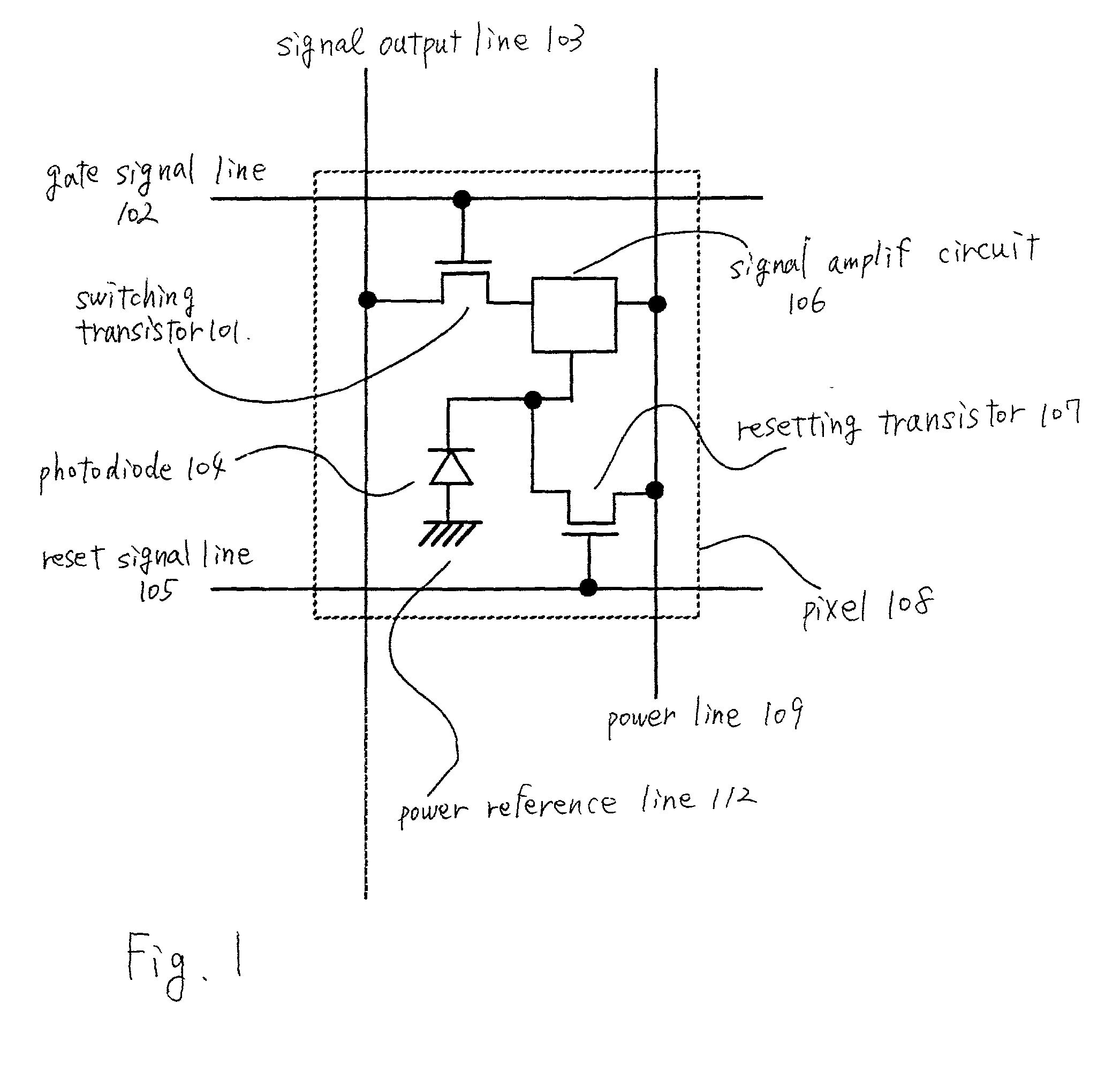
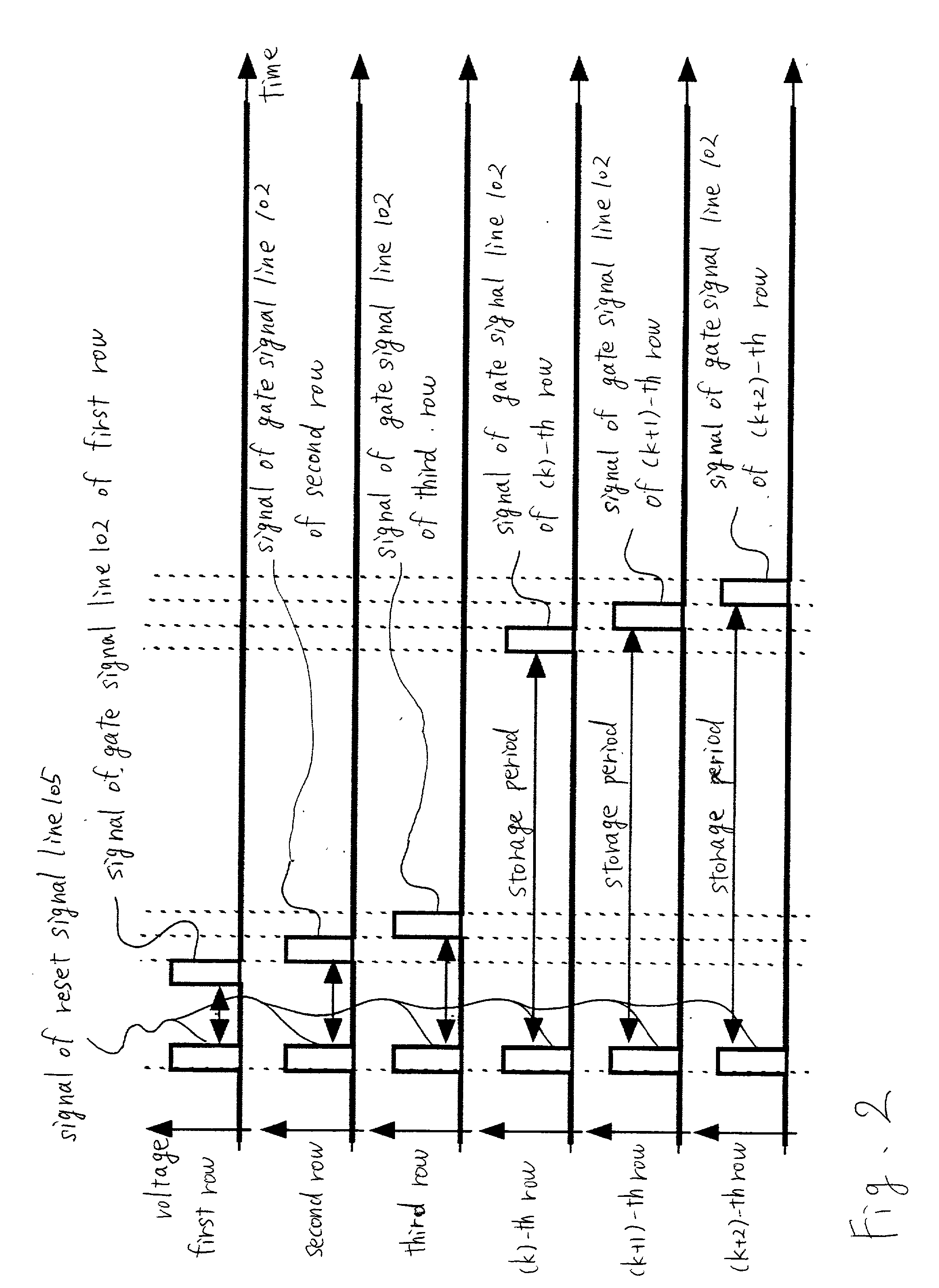
MOS sensor and drive method thereof
a sensor and drive method technology, applied in the direction of radio frequency control devices, instruments, television systems, etc., can solve the problems of low power consumption, partial spreading, destructive reading of passive sensors,
- Summary
- Abstract
- Description
- Claims
- Application Information
AI Technical Summary
Problems solved by technology
Method used
Image

Examples
embodiment 5
[0298] The sensor formed by implementing the present invention can be used in various electronic apparatus. As such electronic apparatus of the present invention, there are pointed out a scanner, a digital still camera, an X-ray camera, a portable information terminal (a mobile computer, a portable telephone, a portable game machine), a note-type personal computer, a game machine, a television telephone and finger print read machine.
[0299] FIG. 29A shows a scanner 2901 using the close contact type sensor and including a sensor unit 2902. The scanner 2901 is arranged above a reading object 2903. The close contact type sensor is fabricated by forming TFTs on a glass substrate. Since the close contact type sensor does not use compact optical system, miniature machines can be achieved. As light for illuminating the reading object 2903, room light is utilized. Thereby, an exclusive light source is not needed. In this case, intensities of light change depending on imaging environment. The...
PUM
 Abstract
Description
Claims
Application Information