

Non-flat liquid crystal display element and method of producing the same
a liquid crystal display element and flat technology, applied in the direction of identification means, signalling systems, instruments, etc., can solve the problems of impeded display operation, impeded flat display element installation on the curved installation surface, impeded display operation, etc., and achieve good display and uniform gap
- Summary
- Abstract
- Description
- Claims
- Application Information
AI Technical Summary
Benefits of technology
Problems solved by technology
Method used
Image

Examples
Embodiment Construction
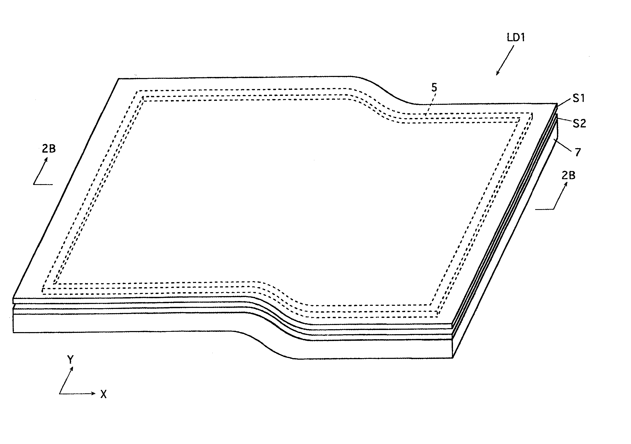
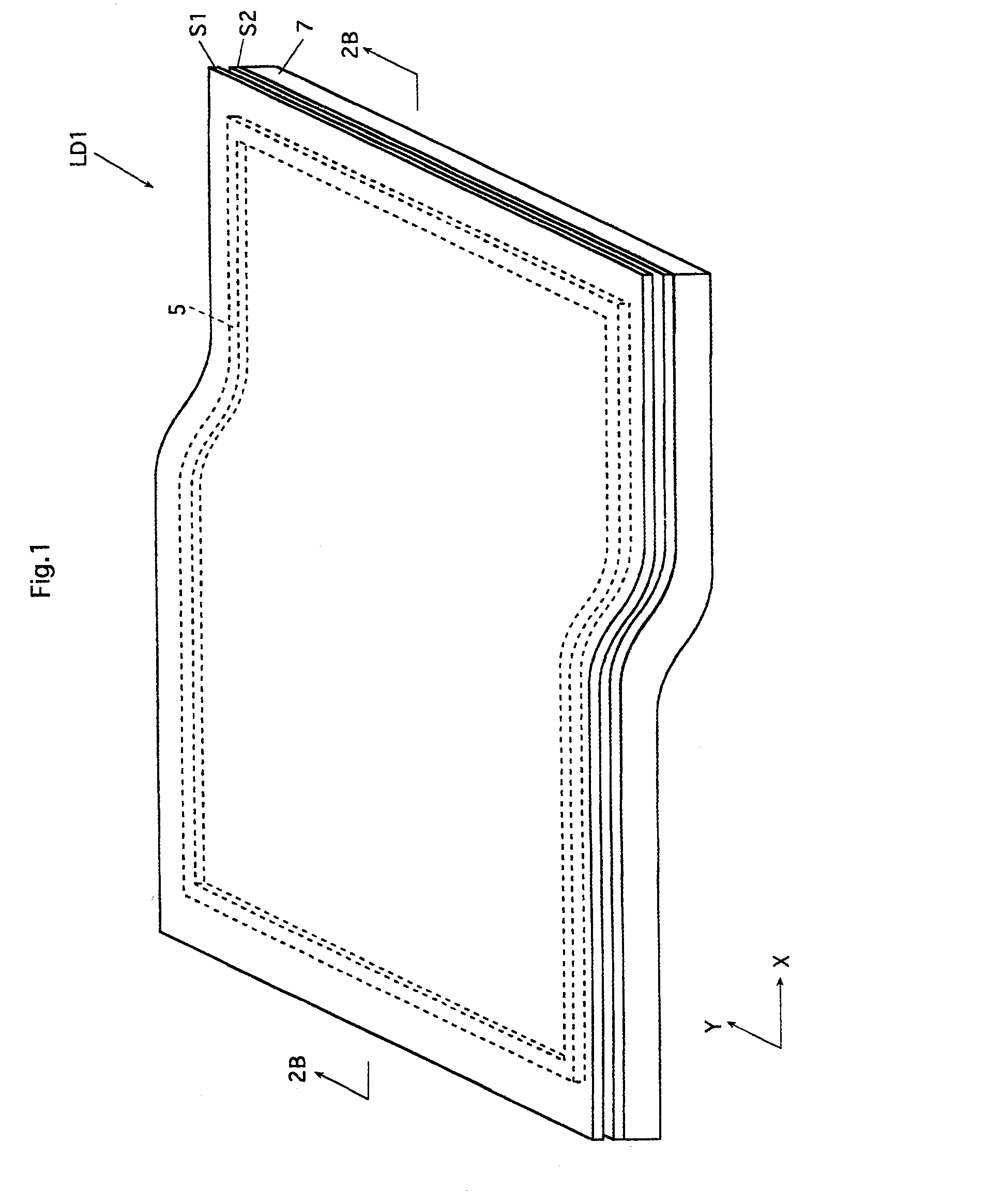
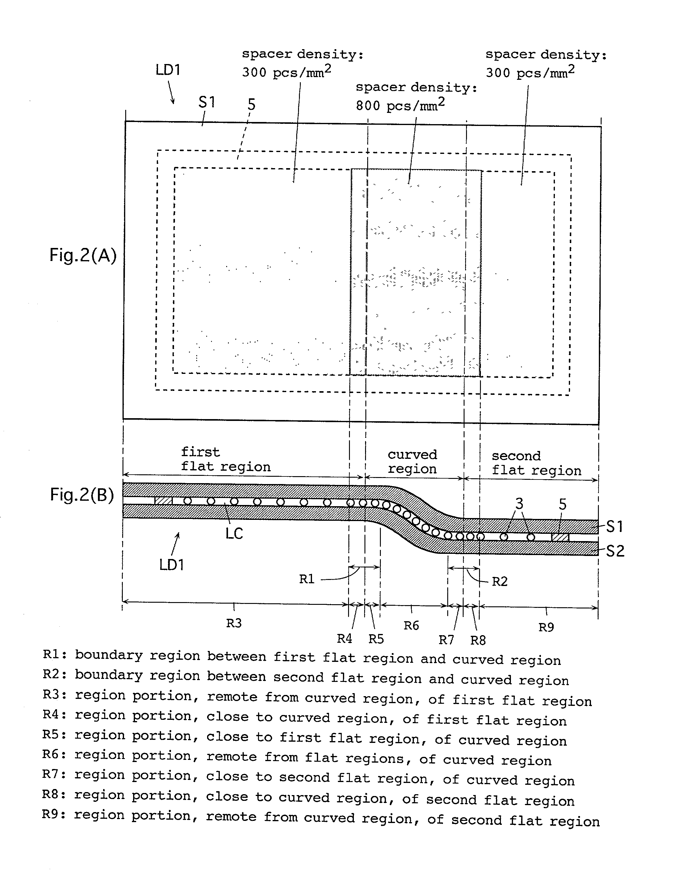
[0085] .sctn.1. Non-Flat Liquid Crystal Display Element
[0086] In the following description, first to eighth types (i.e., eight types) of non-flat liquid crystal display elements are presented.
[0087] In this specification, the non-flat liquid crystal display element may have (1) a curved form having a single curvature, (2) a plurality of regions of different curvatures or (3) a plurality of flat regions of which normals extend in different directions. The non-flat liquid crystal display element of the above (2) may further have a flat region. The curved region of the non-flat liquid crystal display element of the above (1) or (2) may have two- or three-dimensional form.
[0088] .sctn.1.1. First to Eighth Types of Non-Flat Liquid Crystal Display Elements
[0089] First, structures and others common to the first to eighth types of the non-flat liquid crystal display elements will be described.
[0090] (a) Each type of the liquid crystal display element has a pair of substrates, a liquid cryst...
PUM
| Property | Measurement | Unit |
|---|---|---|
| thickness | aaaaa | aaaaa |
| thickness | aaaaa | aaaaa |
| particle diameter | aaaaa | aaaaa |
Abstract
Description
Claims
Application Information