Light-emitting device and electronic devices

a technology of light-emitting devices and electronic devices, which is applied in the direction of static indicating devices, discharge tubes luminescnet screens, instruments, etc., can solve the problems of increasing the number of components, increasing the weight of electronic devices, and increasing the complexity of electronic devices, so as to achieve high contrast

Inactive Publication Date: 2005-06-16
SEMICON ENERGY LAB CO LTD
View PDF30 Cites 146 Cited by
  • Summary
  • Abstract
  • Description
  • Claims
  • Application Information

AI Technical Summary

Benefits of technology

[0010] However, in the case where a main screen and a sub screen are displayed by providing such a plurality of overlapped panels as described above, an electronic device has become heavy and thick. In addition, driver circuits or FPCs for two panels, that is, the main screen and the sub screen, are required, and the number of components are increased; therefore, a structure of the electronic device is more complicated.
[0044] The invention can solve a problem of difficulties in displaying in black in a dual emission type display device, and enhance contrast by displaying in black more favorably by using a polarizing plate or a circularly polarizing plate.

Problems solved by technology

However, in the case where a main screen and a sub screen are displayed by providing such a plurality of overlapped panels as described above, an electronic device has become heavy and thick.
In addition, driver circuits or FPCs for two panels, that is, the main screen and the sub screen, are required, and the number of components are increased; therefore, a structure of the electronic device is more complicated.

Method used


Image

  • Light-emitting device and electronic devices
  • Light-emitting device and electronic devices
  • Light-emitting device and electronic devices

Examples


embodiment mode 1

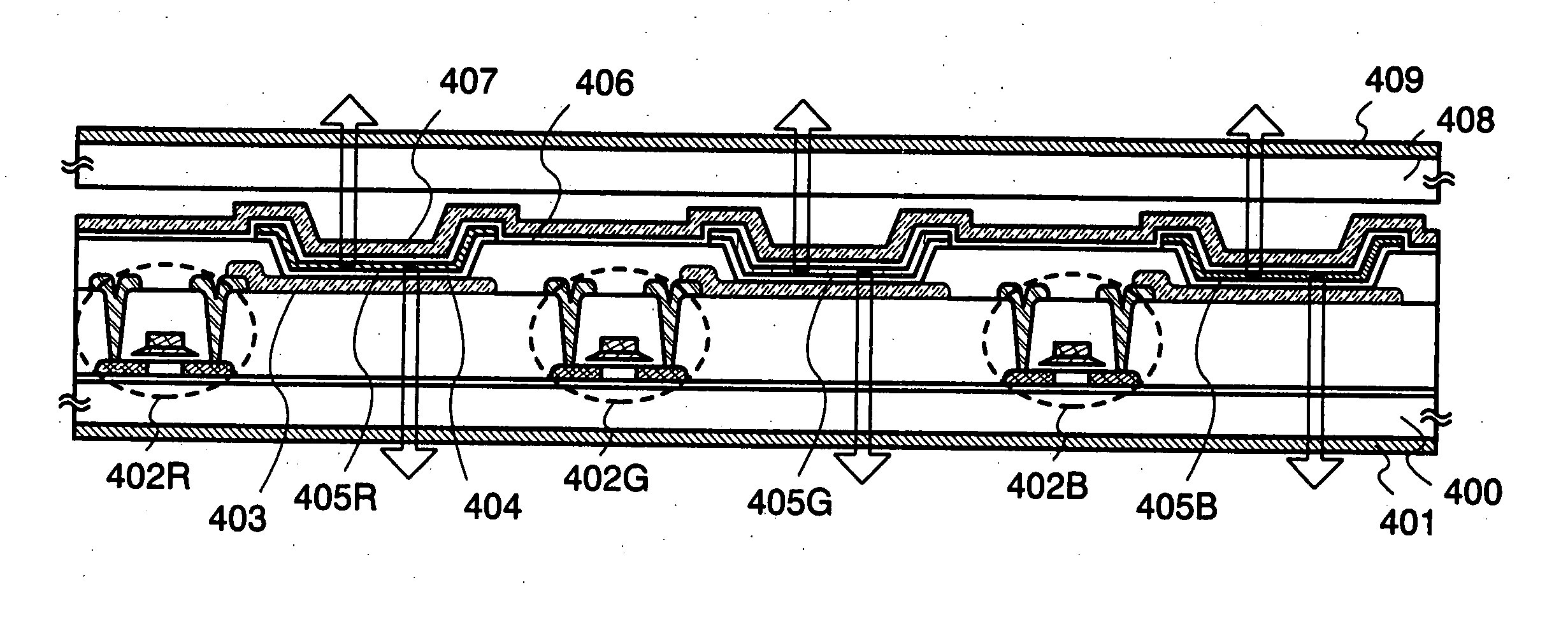
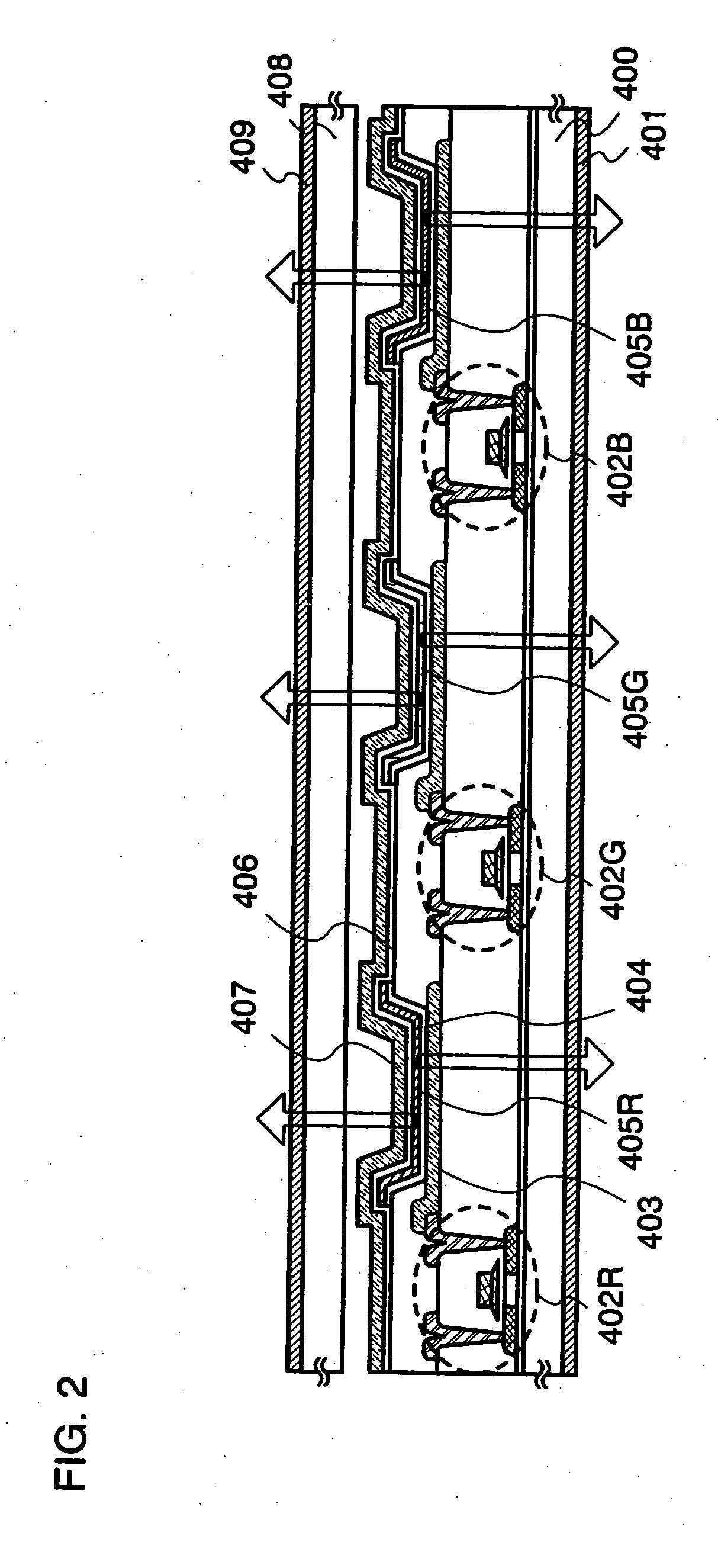
[0066] A method for manufacturing a dual emission type display device is described with reference to FIG. 2.

[0067] A base insulating film is formed over a substrate 400 first. In the case of extracting light by using a substrate side as one display surface, a light-transmitting glass substrate or quartz substrate may be used as the substrate 400. In addition, a light-transmitting plastic substrate that is heat-resistant enough to withstand a processing temperature may be used. Herein, a glass substrate is used as the substrate 400. Note that a refractive index of the glass substrate is approximately 1.55.

[0068] A base film made of an insulating film such as a silicon oxide film, a silicon nitride film, or a silicon oxynitride film is formed as the base insulating film. Note that the base insulating film is also light-transmitting. Although the base film has a two-layer structure here, it may have a single layer structure or a laminated structure of two or more layers of the above ...

example 1 of experiment

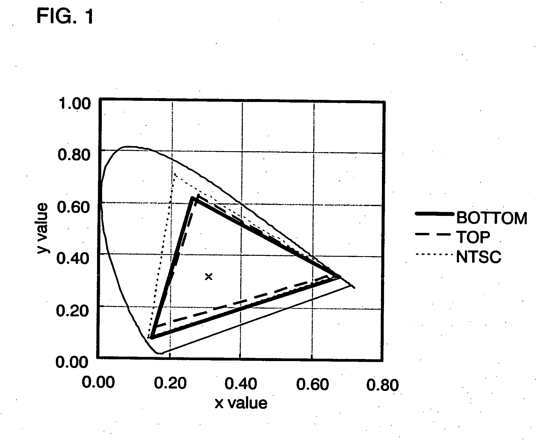
[0100] In this embodiment mode, the transmittance in the case of using a combination of polarizing plates using a metal halide lamp IMH-250 (manufactured by SIGMA KOKI) as a light source is evaluated. Reference of this experiment is air.

[0101] The arrangement conditions of polarizing plates are shown below. The arrangement conditions is an order from a light-source. Condition 1: polarizing plate A and polarizing plate B.

[0102] Angular dependency of the polarizing plates A and B arranged as Condition 1 is measured in this embodiment mode. The result is shown below.

[0103] First, the polarizing plates A and B are arranged at a 90° angle as crossed nicols and the state is an angular deviation of 0°. Then, the relation between transmitted light and the angular deviation of the optical axis of the polarizing plate A from the crossed nicols in a measurement system in FIG. 5 is shown in Table 1. Further, in Table 1, luminance of the transmitted light is normalized as 1 by the value of pa...

example 2 of experiment

[0106] Here, an experiment for evaluating reflected light using a polarizing plate or various circularly polarizing plates by using a metal halide lamp IMH-250 (manufactured by SIGMA KOKI) as a light source is performed.

[0107] First, Samples made under the conditions shown below are prepared. The number shown in ( ) is an angle formed between a transmission axis (0°) of a polarizing plate and a slow axis of a wave plate. [0108] Condition 1: glass substrate+metal film [0109] Condition 2: glass substrate+metal film+polarizing plate [0110] Condition 3: glass substrate+metal film+quarter-wave plate (45°)+polarizing plate [0111] Condition 4: glass substrate+metal film+quarter-wave plate (80°)+half-wave plate (17.5°)+polarizing plate [0112] Condition 5: glass substrate+metal film+quarter-wave plate (45°)+half-wave plate (45°)+polarizing plate [0113] Condition 6: glass substrate+metal film+half-wave plate (45°)+polarizing plate

[0114] In this experiment, reference of this experiment is ai...


PUM


Abstract

The present invention provides a light-emitting device having a new structure which has a plurality of display screens and further achieves lightweight and thinning. Further, the invention provides a dual emission type display device which can perform a pure black display and can achieve high contrast. According to the invention, at least, both electrodes of a light-emitting element (an anode and a cathode of a light-emitting element) are highly light-transmitting at the same level, and a polarizing plate or a circularly polarizing plate is provided, thereby conducting a pure black display that is a state of no light-emission and enhancing the contrast. Moreover, unevenness of color tones in displays of the both sides, which is a problem of a new structure, namely, a full-color dual emission type display device, can be solved according to the invention.

Description

BACKGROUND OF THE INVENTION [0001] 1. Field of the Invention [0002] The present invention relates to a light-emitting device using a light-emitting element that can produce fluorescence or phosphorescence by applying an electric field to the element provided with a film containing organic compound (hereinafter, also referred to as an organic compound layer) between a pair of electrodes and a manufacturing method thereof. Specifically, the invention relates to a light-emitting device in which light-emitting elements are arranged in active matrix form, and light generated in the light-emitting element is emitted to opposite sides. [0003] 2. Description of the Related Art [0004] In recent years, research relating to a light-emitting device having an EL (electroluminescent) element as a self-luminous type light-emitting element has been advanced actively. The light-emitting device is referred to as an organic EL display or an organic light-emitting diode. Since these light-emitting devi...

Claims


Application Information

Patent Timeline
Patent Type & Authority Applications(United States)
IPC IPC(8): G09G3/30H01L27/32H05B33/12H01L51/50H01L51/52H05B33/00H05B33/02H05B33/14H05B33/22H05B33/26H05B33/28H05B44/00
CPCH10K59/35H10K59/12H10K50/86H10K2102/3031H05B33/22
Inventor YAMAZAKI, SHUNPEIHIRAKATA, YOSHIHARUISHITANI, TETSUJINAKAMURA, YASUOIKEDA, HISAOOHARA, HIROKI
Owner SEMICON ENERGY LAB CO LTD
Why Eureka
Try Eureka