Magnetoresistive film having non-magnetic spacer layer of reduced thickness

a non-magnetic spacer layer and magnetoresistive film technology, applied in the field of magnetoresistive elements, can solve the problems of increased shunt current in the magnetoresistive film, inability to contribute to the detection of variation in the electric resistance and the exposed surface of the magnetoresistive film suffers from so-called interfacial roughness

Inactive Publication Date: 2002-06-27
FUJITSU LTD
View PDF5 Cites 3 Cited by
  • Summary
  • Abstract
  • Description
  • Claims
  • Application Information

AI Technical Summary

Problems solved by technology

In this case, the exposed surface of the magnetoresistive film suffers from a so-called interfacial roughness in the heat treatment.
However, the increased thickness of the non-magnetic spacer layer leads to an increased shunt current in the magnetoresistive film.
Such a shunt current cannot contribute to detection of variation in the electric resistance of the magnetoresistive film.
Moreover, a smaller thickness of the non-magnetic space

Method used


Image

  • Magnetoresistive film having non-magnetic spacer layer of reduced thickness
  • Magnetoresistive film having non-magnetic spacer layer of reduced thickness
  • Magnetoresistive film having non-magnetic spacer layer of reduced thickness

Examples


Embodiment Construction

.7 99.5 0.4 Comparative Example 4 87.5 6.5

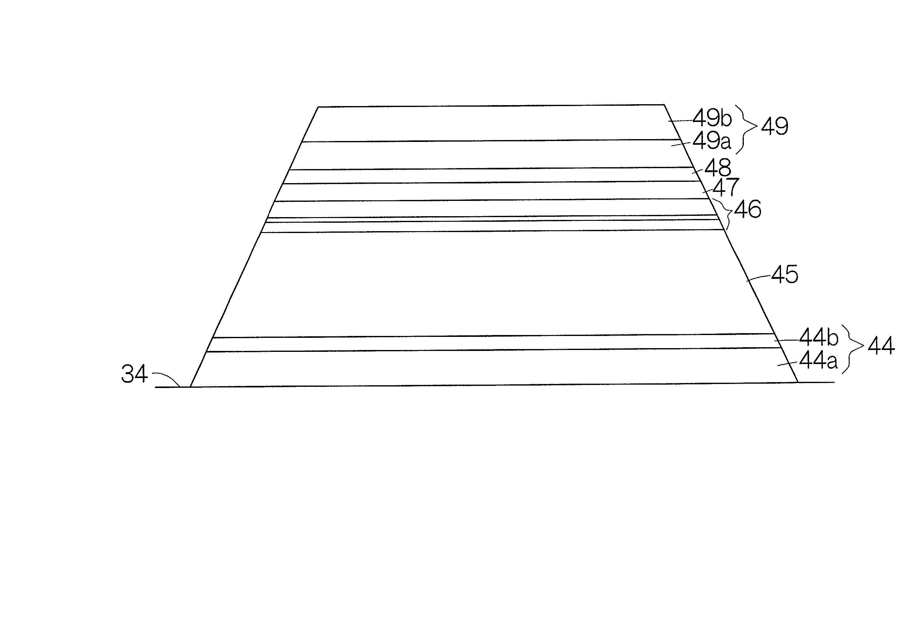
[0060] As is apparent from Table 2, it has been confirmed that the specific example of the spin valve film 41 achieves a remarkably smaller exchange coupling Hin between the pinned ferromagnetic layer 46 and the free ferromagnetic layer 48, as compared with the comparative example, while it exhibits the exchange coupling Hua, similar to that of the comparative example, between the first and second pinned ferromagnetic layers 46a, 46c. This results in a larger magnetoresistive ratio in the specific example.

[0061] Furthermore, the inventors prepared another specific examples of the aforementioned spin valve film 41. These specific examples were designed to include a Ta layer of 5. Onm thickness, an NiFe layer of 2. Onm thickness, a PdPtMn layer of 15. Onm thickness, a CoFeB layer of 1.0 nm thickness, an Ru layer of 0.7 nm thickness, a CoFeB layer of 1.5 nm thickness, a Cu layer as the non-magnetic spacer layer 47, a CoFeB layer of 2.0 nm thick...


PUM


Abstract

A first pinned ferromagnetic layer, an antiferromagnetic bonding layer and a second pinned ferromagnetic layer are sequentially formed over an antiferromagnetic layer. A layered ferrimagnetic structure is established. A compound or oxide layer is interposed between the antiferromagnetic bonding layer and the second pinned ferromagnetic layer. The compound layer serves to efficiently prevent transmission of an undulation or interfacial roughness. Undulation or interfacial roughness can be suppressed at the interface or boundary of a non-magnetic spacer layer formed on the second pinned ferromagnetic layer. The magnetic interaction can thus be suppressed between the second pinned ferromagnetic layer and a free ferromagnetic layer on the non-magnetic spacer layer, irrespective of a smaller thickness of the non-magnetic spacer layer. The magnetization of the free ferromagnetic layer can thus easily rotated in response to the polarity of an applied magnetic field, irrespective of a smaller thickness of the non-magnetic spacer layer. The magnetoresistive ratio can be improved.

Description

Field of the Invention[0001] The present invention relates to a magnetoresistive element in general utilized to read a magnetic information or binary data out of a magnetic recording medium such as a magnetic disk and a magnetic tape. In particular, the invention relates to a magnetoresistive film comprising: an antiferromagnetic layer; a first pinned ferromagnetic layer formed to extend on the antiferromagnetic layer; an antiferromagnetic bonding layer formed to extend on the first pinned ferromagnetic layer; a second pinned ferromagnetic layer formed to extend on the antiferromagnetic bonding layer; a non-magnetic spacer layer formed to extend on the second pinned ferromagnetic layer; and a free ferromagnetic layer formed to extend on the non-magnetic spacer layer, and a method of making the same.Description of the Prior Art[0002] In general, a method of making an antiferromagnetic layer includes a heat treatment effected on a material layer containing an antiferromagnetic metalli...

Claims


Application Information

Patent Timeline
IPC IPC(8): G11B5/39G01R33/09H01F10/08H01F10/26H01F10/32H01F41/28H01F41/30H01L43/08H01L43/12
CPCB82Y10/00B82Y25/00B82Y40/00G11B5/3903G11B5/3967Y10T428/1107H01F10/3272H01F10/3277H01F41/307H01L43/08H01F10/3268H10N50/10G11B5/39
Inventor SHIMIZU, YUTAKASHIBATA, TATSUMA
Owner FUJITSU LTD
Why Eureka
Try Eureka