Hermetic package for mems devices with integrated carrier

a technology of integrated carrier and electronic components, applied in the field of microelectromechanical systems (mems), can solve the problems of smaller chips, complicated electronic devices, and difficult interconnection of various components of modern electronic devices

Inactive Publication Date: 2002-07-11
3M INNOVATIVE PROPERTIES CO
View PDF0 Cites 46 Cited by
  • Summary
  • Abstract
  • Description
  • Claims
  • Application Information

AI Technical Summary

Problems solved by technology

As modern electronic devices have become more complicated, it has also become more difficult to interconnect their various components.
The smaller size of the chips creates a problem when trying to provide connections between the chip leads and external devices or leads, such as those on a printed circuit board (PCB).
Minor errors in the placement of these chips can accordingly result in mis-connection, leading to nonfunctional units, and oftentimes damage to sensitive electrical circuits within the chips.
These problems can be compounded on multi-chip modules (MCMs).
Third, it provides electrical connections from the chip to the system in which it is installed.
Unlike conventional mechanical devices, MEMS devices can be monolithically integrated with integrated circuitry, while providing much improved insertion loss and electrical isola...

Method used


Image

  • Hermetic package for mems devices with integrated carrier
  • Hermetic package for mems devices with integrated carrier
  • Hermetic package for mems devices with integrated carrier

Examples


Embodiment Construction

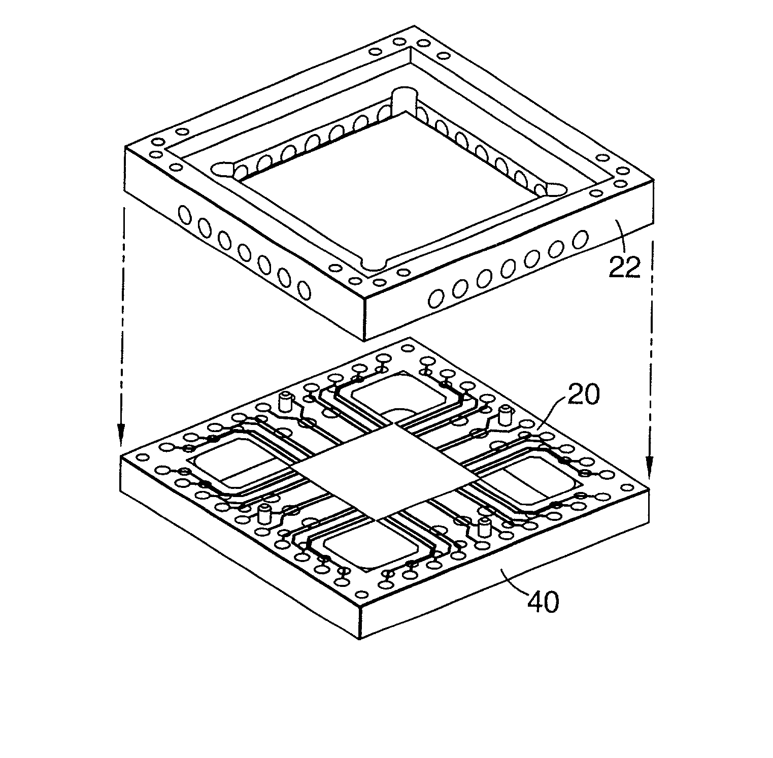
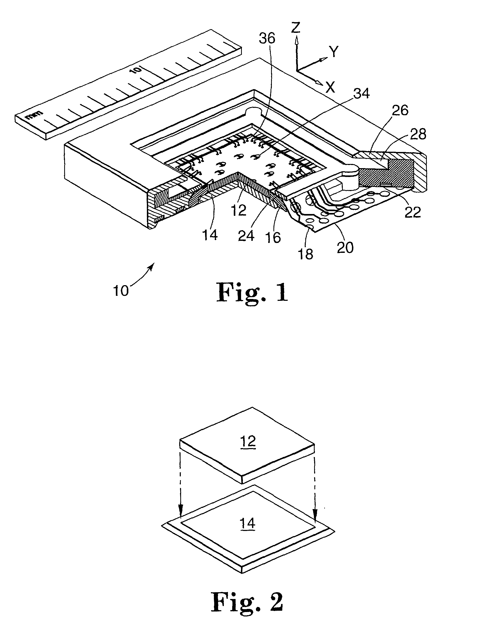
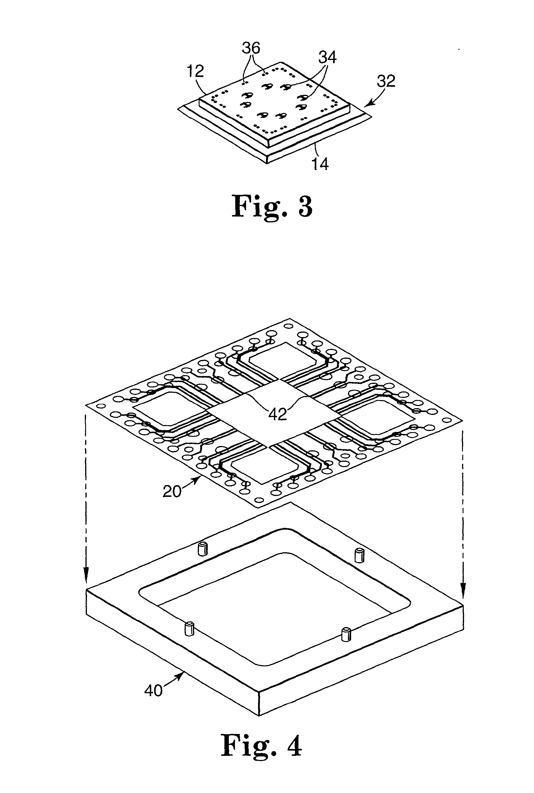
[0046] With reference now to the figures, and in particular with reference to FIG. 1, there is depicted one embodiment 10 of a packaged MEMS device constructed in accordance with the present invention. MEMS package 10 is generally comprised of a MEMS die 12, a carrier 14, a carrier insert 16, a ball grid array pad 18, a flex circuit substrate 20, a pad insert 22, a cover insert 24, and an outer body 26. MEMS package 10 also includes a cover which, although preferably transparent, is not shown in order to see the other elements of the package. The cover is retained in slot 28 formed between pad insert 22 and outer body 26.

[0047] The preferred method of fabricating package 10 is illustrated in FIGS. 2-12. The method begins with the pre-processing of MEMS die 12 as shown in FIGS. 2 and 3. A standard die-attach machine can be used to perform the placement of MEMS die 12 onto carrier 14, since the MEMS mechanisms are encased in their sacrificial oxide (i.e., unreleased). Standard die-att...


PUM


Abstract

A method of fabricating a package for a micro-electromechanical systems (MEMS) device. A flex circuit interconnect subassembly for the package is made by placing a flex circuit on a pad insert, attaching a carrier insert to the pad insert to deflect the lead portions of the flex circuit, and applying a cover insert to the pad insert, after the attachment of the carrier insert, to re-deflect the lead portions of the flex circuit toward the device bond sites. The flex circuit interconnect subassembly may be combined with an electronic device die/carrier subassembly to form a completed electronic device package. The flex circuit interconnect subassembly and the die/carrier subassembly are joined using mechanical interlocking layers. The invention is particularly suited for making such an electronic device die/carrier subassembly which has a MEMS die permanently affixed to a carrier. The carrier is advantageously utilized during the process of releasing a protective coating from the surface of the MEMS die which support the various MEMS components. The MEMS components on the MEMS die are hermetically sealed, such as by bonding a cover to the upper package body or the lower package body. The cover may have features such as ports which allow the MEMS components to interact with the external environment.

Description

[0001] This application is related to U.S. patent application Ser. No. ___ / ___ entitled "MEMS PACKAGE WITH FLEXIBLE CIRCUIT INTERCONNECT" (attorney docket no. 56257USA5A.002), and U.S. patent application Ser. No. ___ / ___ entitled "HERMETIC MEMS PACKAGE WITH INTERLOCKING LAYERS" (attorney docket no. 56259USA1A.002), both of which are filed concurrently herewith and which are hereby incorporated.[0002] 1. Field of the Invention[0003] The present invention generally relates to the interconnection of electronic components, particularly micro-electromechanical systems (MEMS), and more specifically to methods of fabricating packages for MEMS devices to provide external electrical connections, e.g., to printed circuit board leads.[0004] 2. Description of Related Art[0005] As modern electronic devices have become more complicated, it has also become more difficult to interconnect their various components. For example, the physical size of microprocessors and integrated circuits (ICs) contin...

Claims


Application Information

Patent Timeline
IPC IPC(8): B81B7/00
CPCB81B7/007H01L2224/48465H01L2224/73265
Inventor SIMMONS, RICHARD L.
Owner 3M INNOVATIVE PROPERTIES CO
Why Eureka
Try Eureka