Flash memory element and manufacturing method thereof

a technology of flash memory and manufacturing method, which is applied in the direction of nanotechnology, electrical equipment, semiconductor devices, etc., can solve the problems of reducing the size of flash memory elements in the prior, flash memory elements cannot afford the same performance, and the retention characteristic of a memory becomes to be bad

Inactive Publication Date: 2003-03-06
SMARTISM CO LTD
View PDF2 Cites 146 Cited by
  • Summary
  • Abstract
  • Description
  • Claims
  • Application Information

AI Technical Summary

Benefits of technology

0024] To achieve the object mentioned above, the present invention presents a flash memory element comprising: a first oxide film formed on a surface of a silicon substrate; a fin active area vertically formed on the first oxide film with a narrow width; a gate tunneling oxide film formed on the top and at both sides of the fin active area; a floating electrode formed on the surfaces of the gate tunneling oxide film and the first oxide film for storing electric charges; a inter-gates oxide film formed on the surface of the floating electrode; and a control electrode formed on the surface of the inter-gates oxide film.

Problems solved by technology

On the other hand, as for an element for flash memory whose scaling down characteristic is not so good, a new manufacturing method and / or a new configuration of an element is required.
The main reason for this demand of new configuration is that there exists some limitation in scaling down the size of an element used for flash memory in the prior art.
A conventional metal-oxide semiconductor(MOS) element can easily restrain a short-channel effect by using a thin gate oxide film according to the scaling down, however, a flash memory element can not afford the same performance.
If the thickness of a tunneling oxide film(14) is less than that, the charges stored in a floating electrode(16) are leaking back to the channel, and thus the retention characteristic of a memory becomes to be bad.
In an SONOS type flash memory element, however, the thickness of oxide-nitride-oxide(ONO) film, which is corresponding to a gate oxide film in a CMOS element, is still thicker than that of the gate oxide film(for example, 2 nm / 4 nm / 4 nm), and thus the scaling down characteristic is worse than that of CMOS element having the same gate length.
Since the trap density is nonuniform, it requires gate length and width over a certain minimum value, and thus it has a limitation in improving its overall integrity.

Method used


Image

  • Flash memory element and manufacturing method thereof
  • Flash memory element and manufacturing method thereof
  • Flash memory element and manufacturing method thereof

Examples


Embodiment Construction

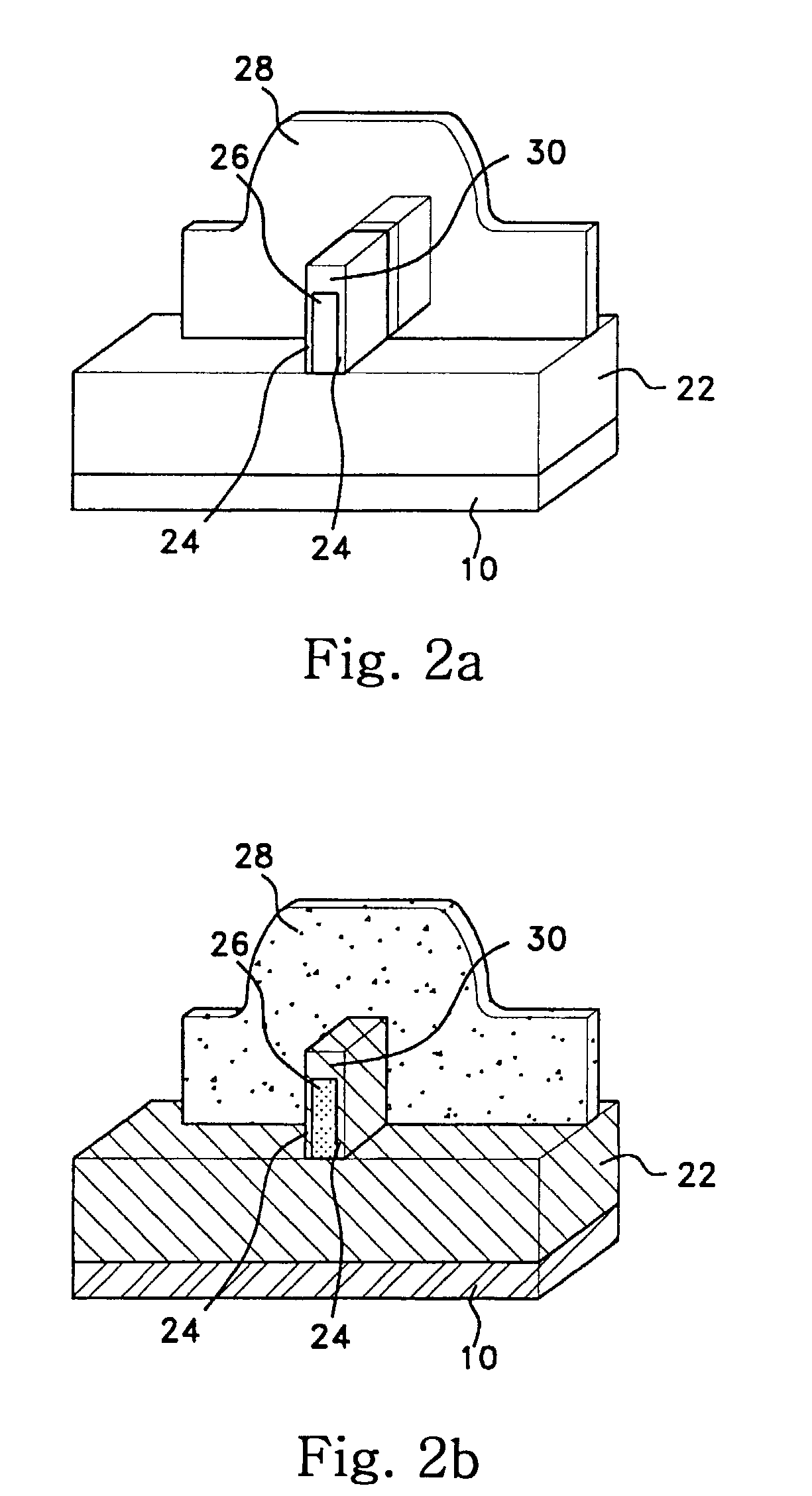
[0051] Hereinafter, referring to appended drawings of FIG. 2a.about.FIG. 6d, the embodiments of the present invention are described in detail.

[0052] First, let us review the structure of a double-gate element constituted on an SOI substrate in the prior CMOS element-related researches for better understanding of the present invention.

[0053] The above-described double-gate element is characterized by the shortest possible channel length among the elements that have been developed up to the present.

[0054] FIG. 2a and FIG. 2b are views illustrating a double-gate element formed on an SOI substrate, wherein the gate is described to be transparent in FIG. 2a and opaque in FIG. 2b.

[0055] The double-gate element is constituted to have gate electrode(28) at both sides(or top and bottom) of a channel, and thus it can considerably improve the so-called short-channel effect.

[0056] Therefore, by applying this concept to scaling down of flash memory element, the element size can be reduced, the i...


PUM


Abstract

The present invention provides a flash memory element and its manufacturing method having improved overall memory characteristics by constituting a double-gate element for improving the scaling down characteristic of flash memory element. A flash memory element comprises: a first oxide film formed on a surface of a silicon substrate; a fin active area vertically formed on the first oxide film; a gate tunneling oxide film formed on the fin active area; a floating electrode formed on the surfaces of the gate tunneling oxide film and the first oxide film; a inter-gates oxide film formed on the surface of the floating electrode; and a control electrode formed on the surface of the inter-gates oxide film. With the above double-gate flash memory structure, a flash memory element in the present invention improves the scaling down characteristic and the programming and retention characteristic of a flash memory element.

Description

[0001] 1. Field of the Invention[0002] The present invention relates to a nano flash memory element and manufacturing method thereof. In more detail, it relates to a flash memory element having improved overall memory characteristics with a double-gate element being constituted therein for improving the scaling down characteristic of flash memory element.[0003] 2. Description of the Related Art[0004] A flash memory is a well-known representative nonvolatile memory and is quite useful for various application fields.[0005] A flash memory is widely used for various electronic instruments as well as for memory itself.[0006] In particular, it has been noticed that flash memory is suitable for the recently being developed embedded logic technology which requires a memory having no processing complexity.[0007] A novel type of high-performance, highly-integrated flash memory can produce a large scale of added-value by being linked to a related logic as well as by memory itself, and thus var...

Claims


Application Information

Patent Timeline
Patent Type & Authority Applications(United States)
IPC IPC(8): H01L21/28H01L21/8247H01L29/423H01L29/788H01L29/792
CPCH01L21/28273H01L29/42324H01L29/785H01L29/7854H01L29/7881H01L29/792H01L29/40114B82Y10/00H10B99/00
Inventor LEE, JONG HOSHIN, HYUNG CHEOL
Owner SMARTISM CO LTD
Why Eureka
Try Eureka