Semiconductor laser device

a laser device and semiconductor technology, applied in the field of semiconductor laser devices, can solve the problems of large strain, large strain, and rapid deformation of laser diodes, and achieve the effect of good thermodynamic stability and higher reliability

Inactive Publication Date: 2003-03-06
FURUKAWA ELECTRIC CO LTD
View PDF0 Cites 15 Cited by
  • Summary
  • Abstract
  • Description
  • Claims
  • Application Information

AI Technical Summary

Benefits of technology

0026] Accordingly, it is an objective of the present invention to provide an active semiconductor layer which has good thermodynamic stability.
0027] It is a further objective of the present invention to enable the construction of semiconductor laser devices which emit light at high output power of 200 mW or more in the 980-nm band and in s

Problems solved by technology

The precipitate creates a localized large strain in the quantum well region due to a large mismatch.
If the strain around the precipitate exceeds a certain amount, dislocation loops appear around the precipitate, and then the laser diode degrades quickly and catastrophic failure occurs.
Thus, the catastrophic failure of thi

Method used


Image

  • Semiconductor laser device
  • Semiconductor laser device
  • Semiconductor laser device

Examples


Embodiment Construction

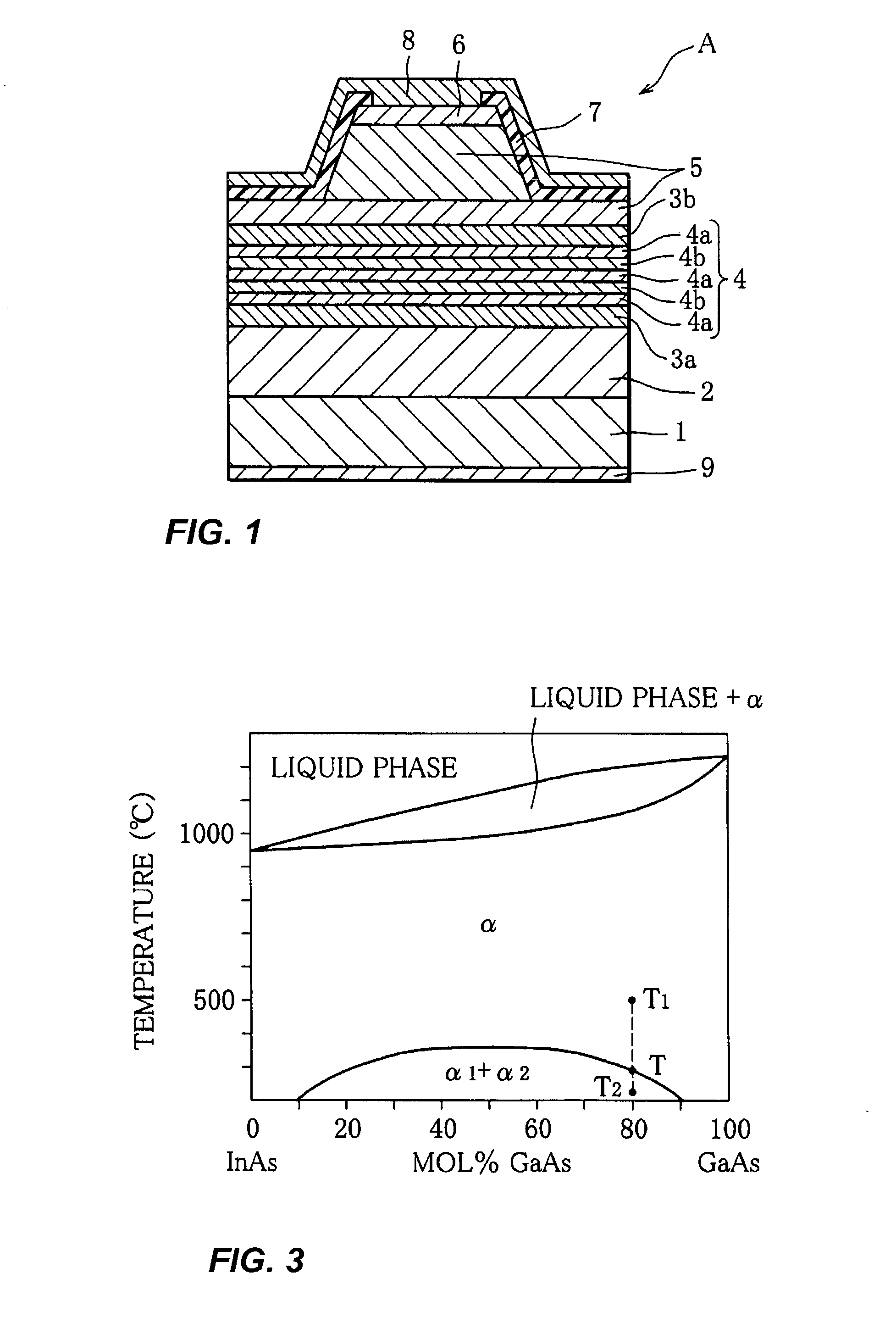
[0178] While the inventors prefer to use an antimony range of 8% to 20% in their 980 nm band pumping lasers, values less than 8% may be used for other emission bands and other device applications. As indicated previously with regard to FIG. 5, for composition values with x between .about.0.03 and .about.0.11, and in the temperature range from 200.degree. C. to 800.degree. C., the material can be thermodynamically stable in either of the solid states (.alpha..sub.1+.alpha..sub.2) and .alpha..sub.2. Thus, when working in this composition range, the growth temperature should be kept below the phase transition line between the (.alpha..sub.1+.alpha..sub.2) and .alpha..sub.2 phases.

[0179] A further embodiment of the present invention comprises an InGaAs quantum well layer grown on a substantially lattice matched InGaAs substrate (indium content generally ranging from 10% to 20%). 980 m emission can be obtained from this system. The phase diagram for InGaAs material system on this ternary...


PUM


Abstract

Disclosed are semiconductor laser devices which hardly have degradation when used to generate high power of 200 mW or greater over a long period of time. An exemplary semiconductor laser device comprising a semiconductor substrate, and a layer structure formed on the semiconductor substrate and having an active layer with a quantum well layer formed of a ternary system mixed crystal of a Ill-V compound semiconductor. The material of the quantum well layer is formed in an equilibrium phase which is thermodynamically stable at both the growth temperature and the operating temperature. The material preferably has a substantially homogeneous disordered microstructure. In a preferred embodiment, the material comprises GaAsSb. The quantum well layer exhibits improved thermodynamic stability, and the device can emit light in the 980 nm band at high power levels for longer periods of time without failure in comparison to conventional InGaAs 980 nm pumping lasers.

Description

[0001] This application is based on Japanese patent application 2001-251,364, filed on Aug. 22, 2001, the whole contents of which are incorporated herein by reference.[0002] The present invention relates to a semiconductor laser device, and, more particularly, to a facet emitting type semiconductor laser device having a Fabry-Perot cavity structure.[0003] Today, most of the laser devices which emit at a wavelength band of 980 nm are made of a GaAs-based compound semiconductor material. The following describes a typical example A of such laser devices referring to FIG. 1.[0004] This laser device A is of a ridge optical waveguide having a Fabry-Perot cavity structure. The laser device A has the following layer structure.[0005] A lower cladding layer 2 of, for example, n-Al.sub.0 3 Ga.sub.0 7As is laminated on a substrate 1 of n-GaAs, followed by a lower SCH layer 3a of, for example, non-doped Al.sub.0 2Ga.sub.0.8As.[0006] A barrier layer 4a of non-doped GaAs.sub.0 9P.sub.0 1 and a wel...

Claims


Application Information

Patent Timeline
IPC IPC(8): H01S3/067H01S5/028H01S5/22H01S5/34H01S5/343
CPCB82Y20/00H01S3/06766H01S3/06775H01S5/0021H01S5/02284H01S5/02438H01S5/028H01S5/0282H01S5/146H01S5/22H01S5/3413H01S5/34306H01S2304/04H01S5/2036H01S5/02251
Inventor YOKOZEKI, MIKIHIROSAITO, KANAMEISHII, HIROTATSUIWAMI, MASAYUKI
Owner FURUKAWA ELECTRIC CO LTD
Why Eureka
Try Eureka