
Apparatus and method for controlling block signal flow in a multi digital signal processor configuration from a shared peripheral direct memory controller to high level data link controller
a technology of block signal flow and multi-digital signal processor, which is applied in the field of data processing systems, can solve the problems of increasing the magnitude and complexity of the application to which the digital signal processor is applied, increasing the need for greater computational power, and inefficient use of semiconductor materials and components
- Summary
- Abstract
- Description
- Claims
- Application Information
AI Technical Summary
Problems solved by technology
Method used
Image

Examples
Embodiment Construction
of the Figures
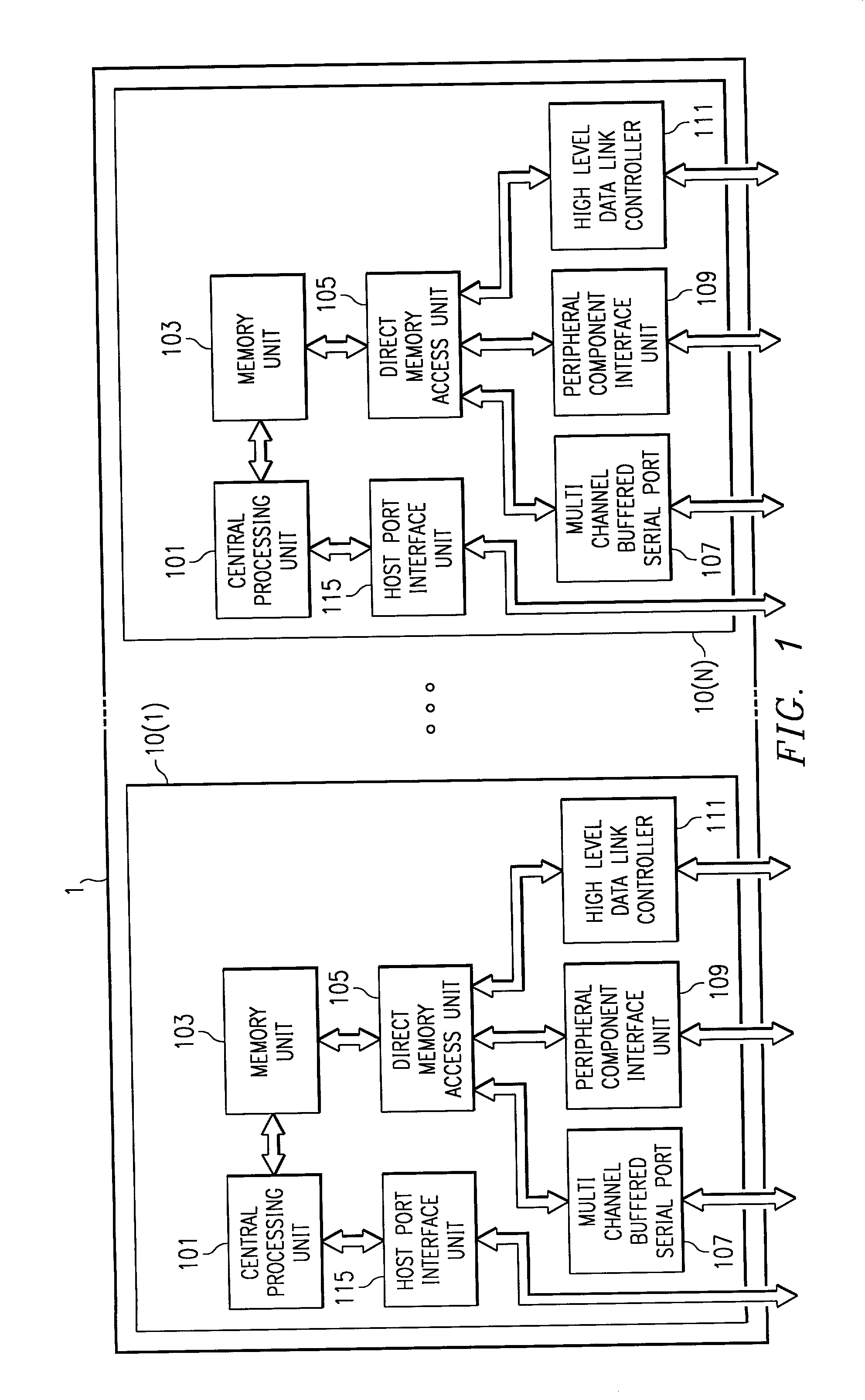
[0015] FIG. 1 has been described with respect to the related art.
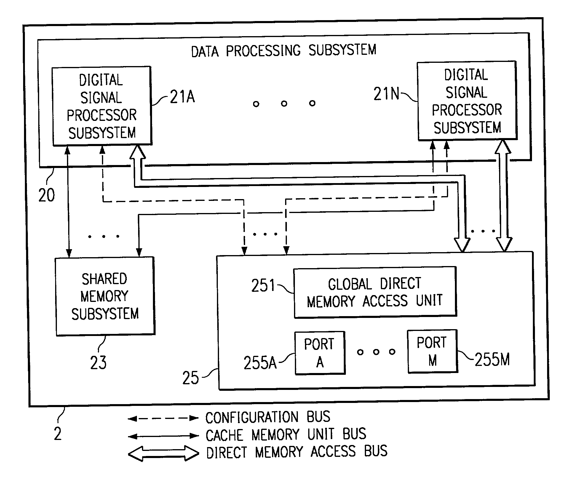
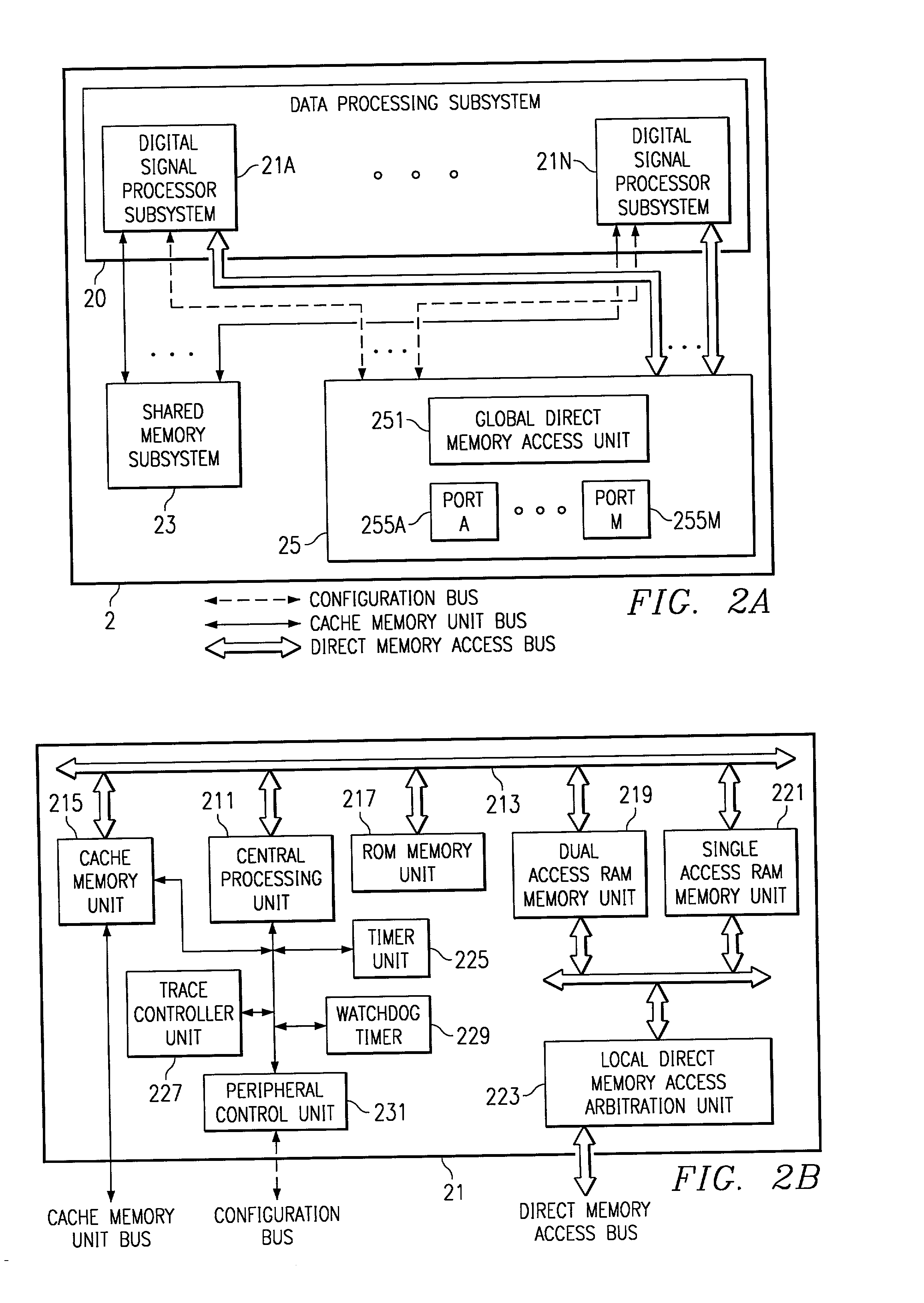
[0016] Referring to FIG. 2A, a block diagram illustrating the subsystems of a data processing system 2 capable of advantageously using the present invention is shown. The data processing system 2 includes a data processing subsystem 20, a shared memory subsystem 23 and a communication subsystem 25. The data processing subsystem 20 includes a plurality of digital signal processing subsystems 21A through 21N. The communication subsystem includes a global direct memory access unit 251 and a plurality of signal exchange ports 25A through 25M. Each digital signal processor subsystem 21A through 21N is coupled to the shared memory subsystem 24 by a cache memory unit bus represented by a solid line. Each digital signal processor subsystem 21A through 21N is coupled to the communication subsystem 25 by a configuration bus represented by a dotted line and each digital signal processor subsystem 21A through 21N is ...
PUM
 Abstract
Description
Claims
Application Information