Active matrix type display device and method of manufacturing the same

a display device and active matrix technology, applied in the direction of organic semiconductor devices, identification means, instruments, etc., can solve the problems of glass substrate breakage, difficult to etch the device forming substrate without damage, and inability to achieve the effect of forming the substrate without damag

Inactive Publication Date: 2003-11-20
JAPAN DISPLAY CENTRAL CO LTD
View PDF1 Cites 71 Cited by
  • Summary
  • Abstract
  • Description
  • Claims
  • Application Information

AI Technical Summary

Problems solved by technology

However, since such a plastic substrate does not have a sufficient heat-resistance or a sufficient dimensional stability, it is not possible to use such a plastic substrate as a device forming substrate on which active elements of polycrystalline silicon, which are superior in switching properties, are formed, and to continuously use the plastic substrate as a supporting substrate.
In the above-described method, however, the process of forming active elements and their wirings on a device forming substrate, which is superior in heat resistance, and then transferring them to, e.g., a plastic substrate, has a problem in the way of removing the device forming substrate used to form the active elements.
For example, in the case where the device forming substrate used to form the active elements should be completely removed, it is difficult to etch the device forming substrate without damaging the active elements on the device forming substrate.
In this display device, if the flexible sheet is bent to form a curved display, it may be possible that the glass substrate breaks.
Therefore, this display device is not reliable when used in a curved application.
As described above, it has been difficult to obtain a reliable and flexible display device without damaging the active matrix devices by first forming active matrix devices and their wirings on a highly heat-resistant device forming substrate, and then transferring them to a flexible plastic substrate.

Method used


Image

  • Active matrix type display device and method of manufacturing the same
  • Active matrix type display device and method of manufacturing the same
  • Active matrix type display device and method of manufacturing the same

Examples


first embodiment

[0060] (First Embodiment)

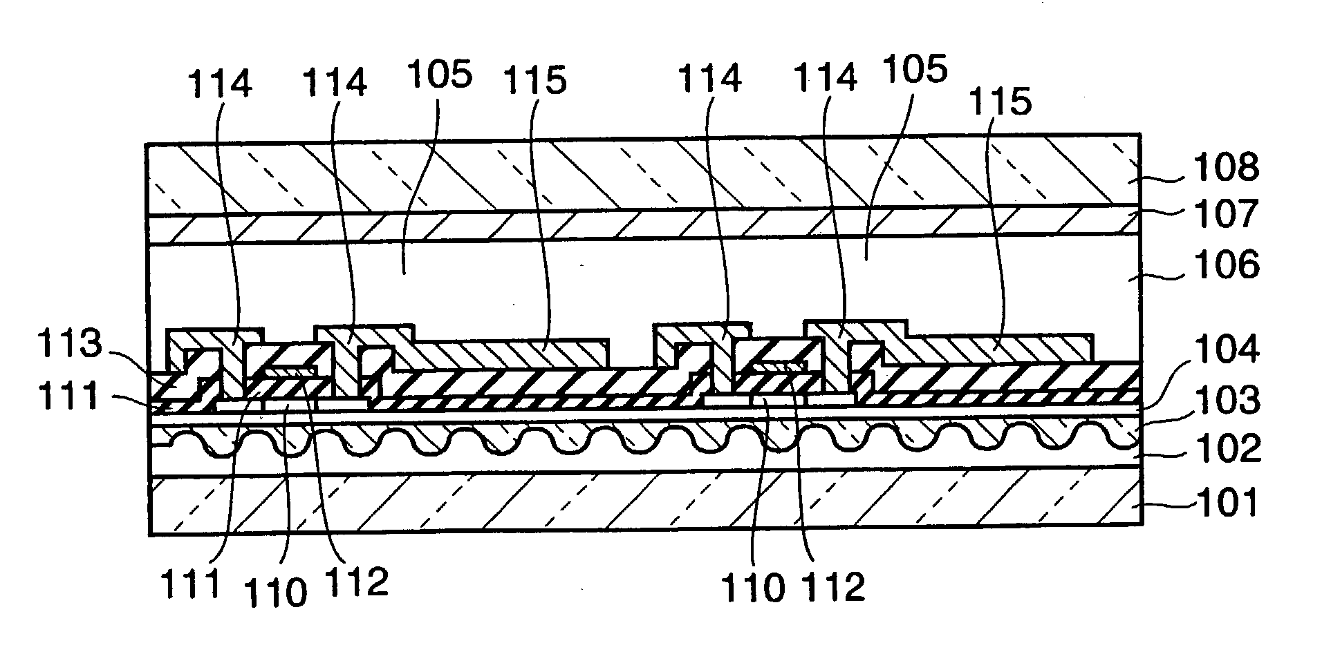
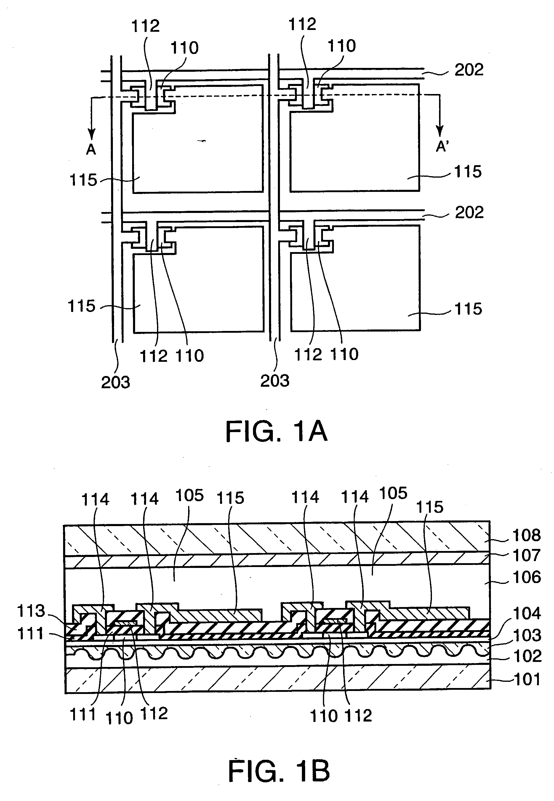
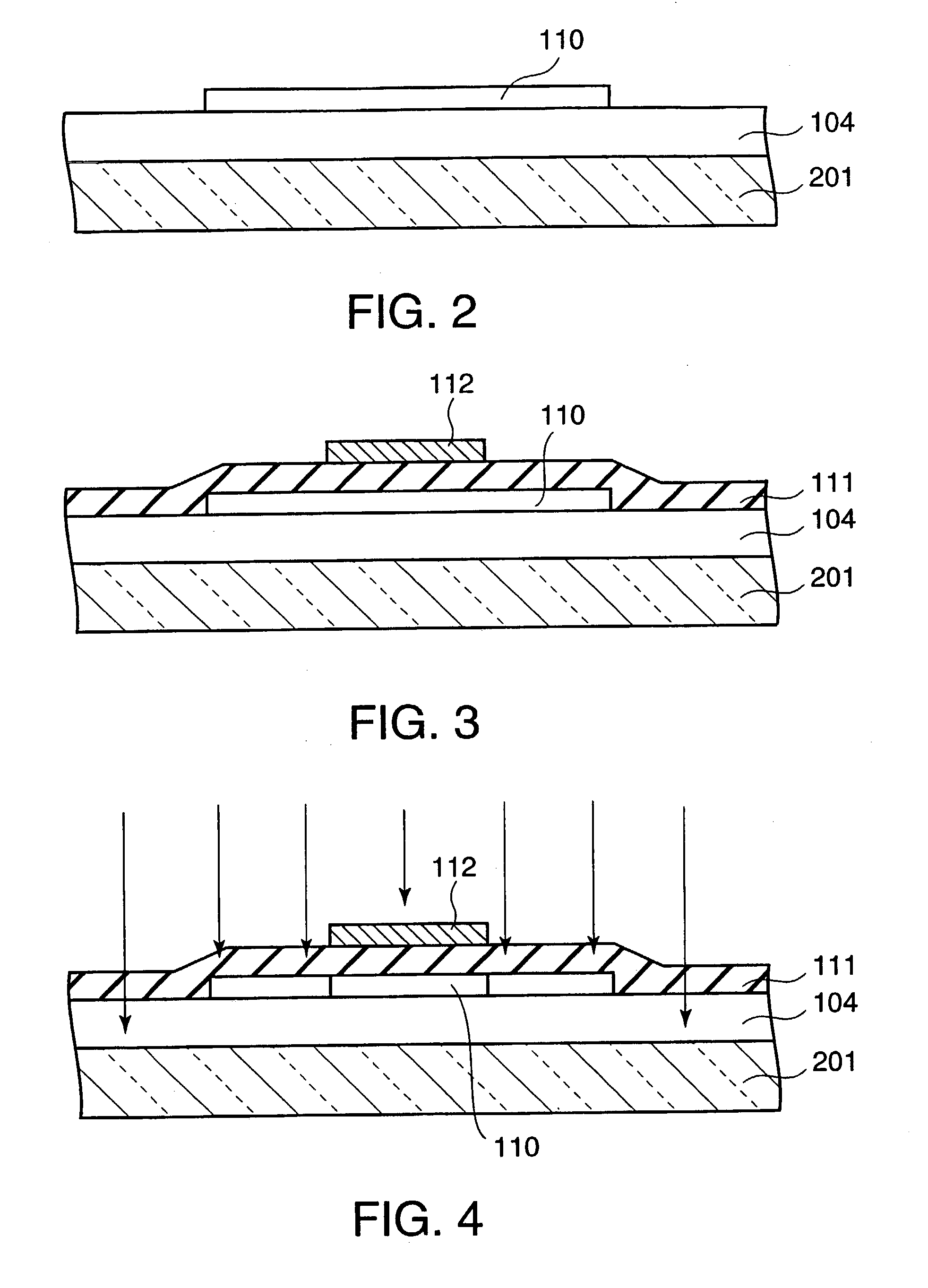
[0061] The first embodiment of the present invention will be described below. FIGS. 1A and 1B show an active matrix type display device in this embodiment. FIG. 1A is a plan view, and FIG. 1B is a sectional view taken on line A-A' of FIG. 1A. FIGS. 2 to 6 are sectional views showing the steps of forming an active element of the active matrix type display device of this embodiment. FIGS. 7 to 10 are sectional views showing the transfer process of the active matrix type display device of this embodiment. It should be noted that although 2.times.2 devices are shown in FIG. 1A, two devices are shown in FIGS. 1B and 7-10, and one device is shown in FIGS. 2-6, actually a great number of such devices are arranged in a two dimensional array.

[0062] In this embodiment, active elements are formed by using a glass substrate as a device forming substrate; the device forming substrate is first mechanically polished, and then chemically polished, thereby making a thin glas...

second embodiment

[0093] (Second Embodiment)

[0094] Next, the second embodiment of the present invention will be described below. FIG. 19 is a sectional view showing an active matrix type display device according to this embodiment. FIGS. 20 to 23 are sectional views showing steps of a method of manufacturing the active matrix type display device of this embodiment. Although two devices are shown in FIG. 19, and one device is shown in FIGS. 20 to 23, in the actual device, a great number of such devices are arranged in a two-dimensional array. With respect to this embodiment, only the features different from those of the first embodiment will be described below, and the descriptions of the same features will be omitted.

[0095] In this embodiment, active matrix devices are formed on a glass substrate serving as a device forming substrate, and then, the thickness of the device forming substrate is reduced to make a thin glass layer. At this time, the thickness of the areas corresponding to at least the ac...

third embodiment

[0107] (Third Embodiment)

[0108] Next, the third embodiment of the present invention will be described below. FIG. 24 is a sectional view showing an active matrix type display device of this embodiment. FIGS. 27 to 29 are sectional views showing the steps of a method of manufacturing the active matrix type display device according to this embodiment. Although only two devices are shown in FIGS. 26 to 29, actually there are a great number of such devices arranged in a two-dimensional array. The details of the thin film transistors are not shown. With respect to this embodiment, only the difference between this embodiment and the first embodiment will be described, and the descriptions on the same features will be omitted.

[0109] In this embodiment, active elements are formed on a glass substrate serving as a device forming substrate. Then, the thickness of the device forming substrate is decreased to form a thin glass layer. Subsequently, a compressive stress applying layer is formed o...


PUM

PropertyMeasurementUnit
temperatureaaaaaaaaaa
thicknessaaaaaaaaaa
thicknessaaaaaaaaaa

Abstract

A method of manufacturing an active matrix type display device, which is reliable and flexible, is provided. An active matrix type display device according to an aspect of the present invention includes: a first substrate, which is flexible; a thin glass layer provided on the first substrate via an adhesion layer, and having projections and depressions on a surface thereof opposing to the first substrate, the projections and depressions having rounded tips and bottoms; active elements provided on the thin glass layer, each active element corresponding to a pixel; a display provided above the thin glass layer, and driven by the active elements to display an image pixel by pixel; and a second substrate provided on the display, and having an opposing electrode formed thereon.

Description

[0001] This application is based upon and claims the benefit of priority from the prior Japanese Patent Application No. 2002-142373, filed on May 17, 2002 in Japan, the entire contents of which are incorporated herein by reference.[0002] 1. Field of the Invention[0003] The present invention relates to an active matrix type display device and a method of manufacturing the same.[0004] 2. Related Art[0005] In an active matrix type display device, which is widely used at present, a highly heat-resistant substrate, e.g., a non-alkali glass substrate, is used as a substrate on which devices are formed during an active element forming process, and the highly heat-resistant substrate is continuously used as a supporting substrate of the display device.[0006] When a thin film transistor is formed by using a polycrystalline silicon layer as a semiconductor layer in which a channel region is formed, the following procedure is employed, taking into consideration the processing temperature etc. ...

Claims


Application Information

Patent Timeline
Patent Type & Authority Applications(United States)
IPC IPC(8): G02F1/1333G02F1/1368G09F9/30H01L21/77H01L21/84H01L27/12H01L27/32H01L29/786H01L51/52
CPCG02F1/133305H01L27/1214H01L27/1266H01L2251/5338H01L29/78603H01L51/52H01L51/5237H01L27/3244H01L27/1218H10K59/12H10K50/80H10K50/841H10K50/8426H10K50/844H10K2102/311G02F1/1333
Inventor HIOKI, TSUYOSHIAKIYAMA, MASAHIKONAKAJIMA, MITSUOHARA, YUJIROONOZUKA, YUTAKA
Owner JAPAN DISPLAY CENTRAL CO LTD
Why Eureka
Try Eureka