Testing liquid crystal microdisplays

a liquid crystal microdisplay and liquid crystal technology, applied in the field of liquid crystal microdisplays, can solve the problems of slow speed in making a complete measurement, lc microdisplays cannot be adjusted, and the light transference characteristics of unconnected pixels cannot be adjusted

Inactive Publication Date: 2003-11-20
BRILLIAN CORP
View PDF5 Cites 51 Cited by
  • Summary
  • Abstract
  • Description
  • Claims
  • Application Information

AI Technical Summary

Problems solved by technology

For example, some devices may have a number of pixels that are not connected for voltage actuation and therefore the light transference characteristics of the unconnected pixels cannot be adjusted.
For another example, the liquid crystal itself may not be properly oriented such that even when voltages are applied, the correct transference characteristics do not occur.
A major drawback to this method of testing LC microdisplays is the slow speed in making a complete measurement.
Still, the repetition of the "show-and grab" takes so long that the time for measurement is prohibitive in production real-time testing.
Accordingly small defects in the display will be enlarged so much that the defects will adversely affect the display quality.
The real challenge in pixel-level defect testing is not in locating or measuring pixel-sized defects.
Rather, the true technical hurdles reside in the measurement of sub-pixel-sized defects that are not much different from the black, white, or gray background employed.
An additional complication originates from the differences between the microdisplay device behavior in the test system compared to operation of the microdisplay in an actual operating application.
There is no known prior production tester that reliably inspects sub-pixel defects for LCOS microdisplays.
Simple increases in the frequency of sampling are insufficient to test sub-pixel defects reliably.

Method used


Image

  • Testing liquid crystal microdisplays
  • Testing liquid crystal microdisplays
  • Testing liquid crystal microdisplays

Examples


Embodiment Construction

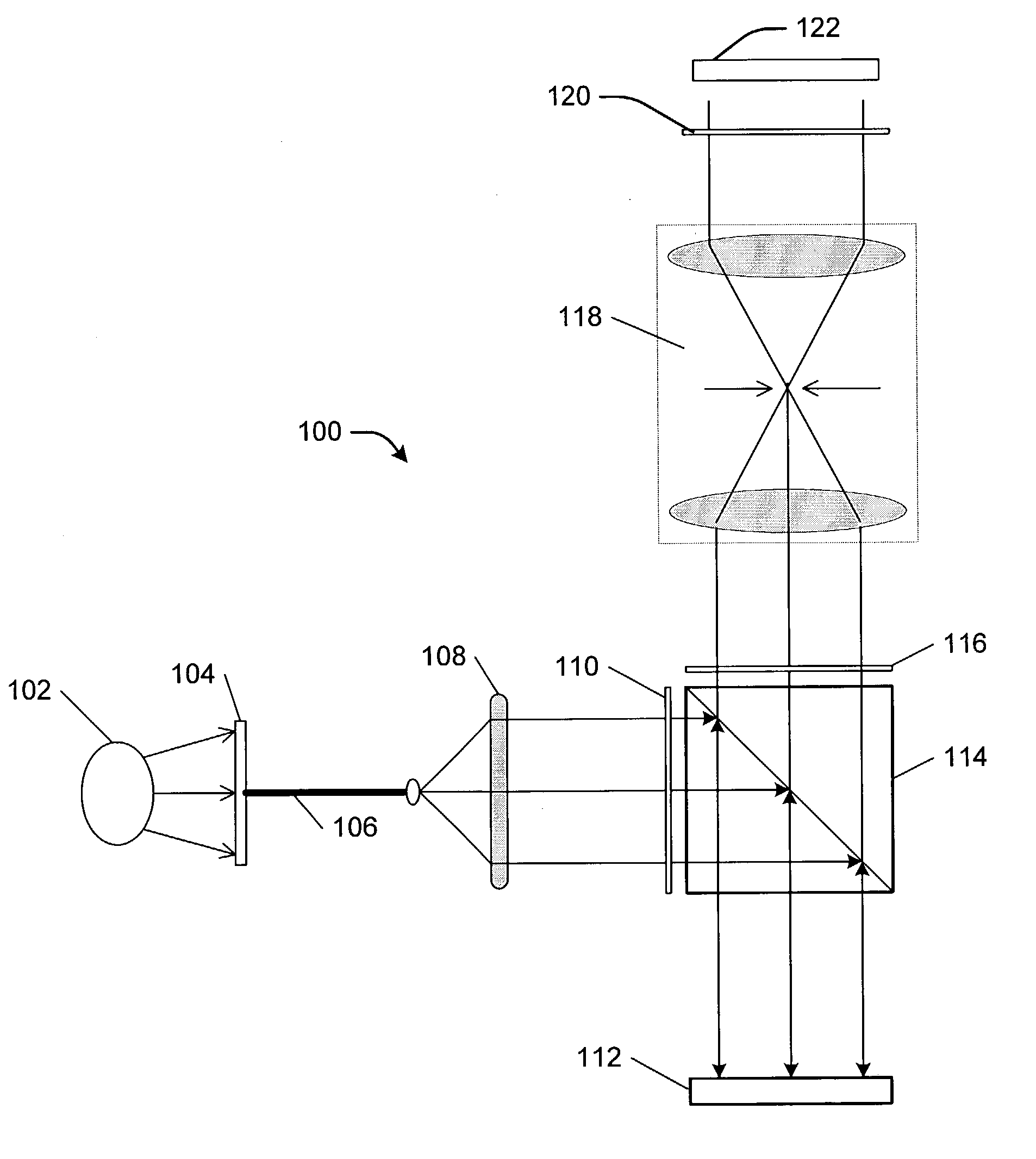
[0039] The present invention is directed to a LC microdisplay test method and system. Another LC microdisplay tester that could benefit from the present invention is more fully described in commonly owned co-pending non-provisional U.S. patent application Ser. No. 10 / 072,456, entitled "System and Method for Testing a Display Device" by Smith et al., filed Feb. 7, 2002, which claimed priority to provisional U.S. patent application Ser. No. 60 / 267,443, filed Feb. 8, 2001, both of which are hereby incorporated by reference herein for all purposes.

[0040] Referring now to the drawings, the details of preferred embodiments of the invention are schematically illustrated. Like elements in the drawings will be represented by like numbers, and similar elements will be represented by like numbers with a different lower case letter suffix.

[0041] Referring to FIG. 1, depicted is a schematic diagram of an optical configuration for a CCD sensor based camera testing system for determining LC microd...


PUM

PropertyMeasurementUnit
sizeaaaaaaaaaa
areaaaaaaaaaaa
pixel sizeaaaaaaaaaa

Abstract

By rendering a special test image and applying flat-field correction for a device under test (DUT) non-uniformity, the E-O response of a reflective LCOS microdisplay can be quickly determined through an image processing algorithm. The measurement is made in a spatial domain instead of in a temporal domain. From the measurement, the driving voltage of maximum brightness, Vbright, can be determined. The use of Vbright enhances the visibility of pixel and sub-pixel defects to the test system. Other defect visibility enhancements are achieved through appropriate sampling rate, optical axis rotation and improved parallelism between the DUT and the CCD sensor camera. By modeling a sub-pixel defect as a local non-uniformity, a near neighborhood algorithm may be used for detection. The neighborhood algorithm does not rely on the alignment between the display pixels and the camera pixels.

Description

RELATED PATENT APPLICATION[0001] This application claims priority, pursuant to 35 U.S.C. .sctn. 119(e), to commonly owned U.S. Provisional Patent Application Serial No. 60 / 380,662, entitled "Method and Algorithm for Fast Mesurement of the Electro-Optical Response for Liquid Crystal on Silicon Microdisplays" by Qingsheng J. Yang, Peter A. Smith and Mathias Pfeiffer, filed May 15, 2002, and is hereby incorporated by reference herein for all purposes.[0002] The present invention relates generally to evaluation of liquid crystal microdisplays, and more particularly to evaluation of the electro-optical (E-O) response of the microdisplay.BACKGROUND OF THE INVENTION TECHNOLOGY[0003] Liquid crystal (LC) displays are commonly used in devices such as portable and large screen projection televisions, portable computers, computer monitors, control displays, and cellular phones to display information to a user. LC displays act in effect as light valves, i.e., they allow transmission of light in ...

Claims


Application Information

Patent Timeline
Patent Type & Authority Applications(United States)
IPC IPC(8): G02F1/13G06T5/00G06T7/00G06T7/40H04N5/74H04N9/30H04N17/00H04N17/04
CPCG02F1/1309G06T7/0002G06T7/0004G06T7/40H04N17/04H04N9/30H04N9/3182H04N9/3194H04N17/00H04N5/7441G01N2021/9513
Inventor YANG, QINGSHENG J.HOFFMAN, DAN D.SMITH, PETER A.PFEIFFER, MATHIAS
Owner BRILLIAN CORP
Why Eureka
Try Eureka