Optimized model and parameter selection for optical metrology

a technology of optical metrology and optimized model, applied in the field of integrated circuit (ic) metrology, can solve the problems of time-consuming and expensive empirical scatterometry technique for building a library, increasing the difficulty of measuring the features of ic devices, and prone to damag

Inactive Publication Date: 2004-01-29
TOKYO ELECTRON US HOLDINGS INC
View PDF15 Cites 89 Cited by
  • Summary
  • Abstract
  • Description
  • Claims
  • Application Information

AI Technical Summary

Benefits of technology

0010] In an exemplary embodiment, a profile model for use in optical metrology of structures in a wafer is selected based on characteristics of the process and/or modeling attributes of the structure included in a template associated with the structure in the wafer. The process includes selecting a template associated with a wafer structure and having one or more parameters including characteristics of process and modeling attributes of the wafer structure. A profile modeling process is then performed to generate a profile model

Problems solved by technology

With the current drive towards smaller geometries of IC devices, measurement of IC device features is increasingly difficult as the size of the features become smaller.
The cross-section SEM method is typically slow, expensive, destructive, and typically only provides one measurement number seen from the top of the feature.
Even for a limited

Method used


Image

  • Optimized model and parameter selection for optical metrology
  • Optimized model and parameter selection for optical metrology
  • Optimized model and parameter selection for optical metrology

Examples


Embodiment Construction

[0042] The following description is presented to enable any person skilled in the art to make and use the invention. Descriptions of specific materials, techniques, and applications are provided only as examples. Various modifications to the examples described herein will be readily apparent to those skilled in the art, and the general principles defined herein may be applied to other examples and applications without departing from the spirit and scope of the invention. Thus, the present invention is not intended to be limited to the examples described and shown, but is to be accorded a scope consistent with the appended claims.

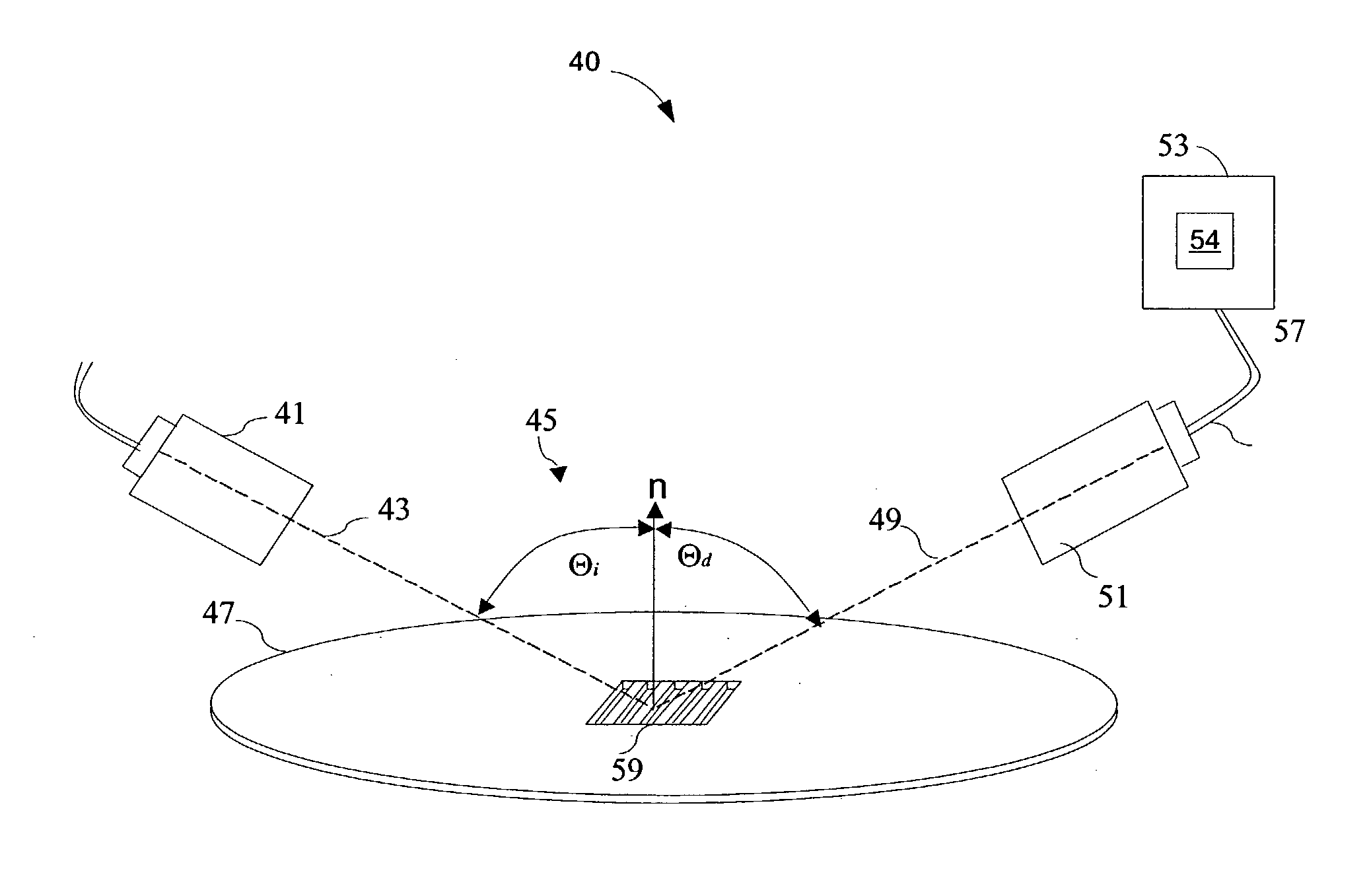
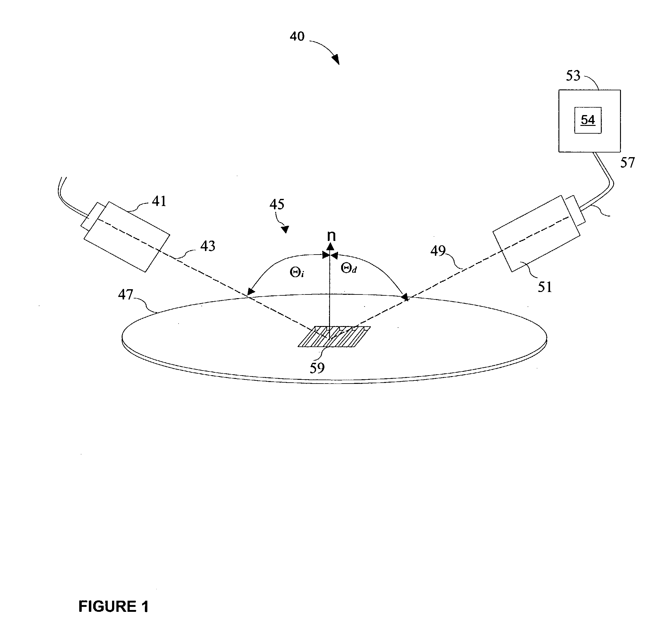
[0043] In order to facilitate the description of the certain aspects of various embodiments, either an ellipsometric or reflectometric optical metrology system is used to illustrate certain concepts and principles. Graphs of diffraction signals off wafer structures using an ellipsometer, e.g., cos (.DELTA.) and tan (.PSI.), will be utilized to describe certa...


PUM


Abstract

A profile model for use in optical metrology of structures in a wafer is selected based on a template having one or more parameters including characteristics of process and modeling attributes associated with a structure in a wafer. The process includes performing a profile modeling process to generate a profile model of a wafer structure based on a template having one or more parameters including characteristics of process and modeling attributes. The profile model includes a set of geometric parameters associated with the dimensions of the structure. The generated profile model may further be tested against termination criteria and the one or more parameters modified. The process of performing a modeling process to generate a profile model and testing the generated profile model may be repeated until the termination criteria are met.

Description

[0001] This application is a continuation-in-part of, and claims benefit to, co-pending U.S. patent application Ser. No. 10 / 206,491, entitled "MODEL AND PARAMETER SELECTION FOR OPTICAL METROLOGY" by Vuong, et al., filed on Jul. 25, 2002, which is incorporated herein by reference.BACKGROUND OF INVENTION[0002] 1. Field of Invention[0003] This application relates generally to integrated circuit (IC) metrology, and more particularly to the selection of a structure model and parameters for optical metrology using a template with expected parameter values and / or value ranges.[0004] 2. Related Art[0005] With the current drive towards smaller geometries of IC devices, measurement of IC device features is increasingly difficult as the size of the features become smaller. One method of measuring the features involves the use of gratings or periodic structures formed in test areas of a wafer that are proximate to or within the devices or circuits on the wafer. Knowledge of the dimensions of th...

Claims


Application Information

Patent Timeline
IPC IPC(8): G01B11/06G01B11/00G01B11/02G01B11/04G01B11/08G01B11/14G01B11/22G01B11/28G01N21/00G01N21/41G01N21/47G06FG06F15/00G06F19/00G06T7/00H01L21/66
CPCG01N21/4788G03F7/705G06T2207/30148G06T7/0006G03F7/70616G03F7/70625
Inventor BALASUBRAMANIAN, RAGHUYEDUR, SANJAYVUONG, VIJAKATDAR, NICKHIL
Owner TOKYO ELECTRON US HOLDINGS INC
Why Eureka
Try Eureka