Memory latency and bandwidth optimizations

a technology of memory latency and bandwidth optimization, applied in the field of memory systems, can solve the problems of slow speed and reliability of the mass storage portion of the computer system, the inability of the computer system to fully capitalize on the increase in the speed of the improving processing system, and the speed of the mass storage device, such as magnetic disk drives, has not improved much

Inactive Publication Date: 2004-04-15
HEWLETT PACKARD DEV CO LP
View PDF7 Cites 67 Cited by
  • Summary
  • Abstract
  • Description
  • Claims
  • Application Information

AI Technical Summary

Problems solved by technology

In contrast to the dramatic improvements of the processing portions of a computer system, the mass storage portion of a computer system has experienced only modest growth in speed and reliability.
As a result, computer systems failed to capitalize fully on the increased speed of the improving processing systems due to the dramatically inferior capabilities of the mass data storage devices coupled to the systems.
While the speed of these mass storage devices, such as magnetic disk drives, has not improved much in recent years, the size of such disk drives has become smaller while maintaining the same or greater storage capacity.
However, it was further recognized that large numbers of smaller disk drives dramatically increased the chance of a disk drive failure which, in turn, increases the risk of data loss.
Of course, a level 1 RAID system requires the cost of an additional disk without increasing overall memory capacity in exchange for decreased likelihood of data loss.
Thus, RAID systems are primarily found in computers performing relatively critical functions where failures are not easily tolerated.
It does not necessarily permit the computer system to be repaired or upgraded without powering down the system.
Although hot plug schemes have been developed for many computer components, including microprocessors, memory chips, and disk drives, most such schemes do not permit the removal and replacement of a faulty device without downgrading system performance to some extent.
Furthermore, in 1998, it was reported that the average cost of a minute of downtime for a mission-critical application was $10,000.00.
In addition to the increasing criticality of such computer systems and the high cost of downtime of such systems, the amount of semiconductor memory capacity of such systems has been increasing steadily and is expected to continue to increase.
Although semiconductor memories are less likely to fail than disk drives, semiconductor memories also suffer from a variety of memory errors.
Specifically, "soft" errors account for the vast majority of memory errors in a semiconductor memory.
Such soft errors include cosmic rays and transient events, for instance, that tend to alter the data stored in the memory.
However, some percentage of these errors are multi-bit errors that are uncorrectable by current ECC technology.
Furthermore, the occurrence of soft errors increases linearly with memory capacity.
Therefore, as memory capacities continue to increase, the number of soft errors will similarly increase, thus leading to an increased likelihood that the system will fail due to a soft error.
Semiconductor memories may also suffer from "hard" errors.
Such hard errors may be caused by over voltage conditions which destroy a portion of the memory structure, bad solder joints, malfunctioning sense amplifiers, etc.
While semiconductor memories are typically subjected to rigorous performance and bum-in testing prior to shipment, a certain percentage of these memories will still malfunction after being integrated into a computer system.
Again, as the number of memory chips and the memory capacities of computer systems increase, a likelihood of a semiconductor memory developing a hard error also increases.
The longer it takes to access memory (access time) and complete a request (cycle time), the slower the performance of the computer system.

Method used


Image

  • Memory latency and bandwidth optimizations
  • Memory latency and bandwidth optimizations
  • Memory latency and bandwidth optimizations

Examples


Embodiment Construction

[0021] One or more specific embodiments of the present invention will be described below. In an effort to provide a concise description of these embodiments, not all features of an actual implementation are described in the specification. It should be appreciated that in the development of any such actual implementation, as in any engineering or design project, numerous implementation-specific decisions must be made to achieve the developers' specific goals, such as compliance with system-related and business-related constraints, which may vary from one implementation to another. Moreover, it should be appreciated that such a development effort might be complex and time consuming, but would nevertheless be a routine undertaking of design, fabrication, and manufacture for those of ordinary skill having the benefit of this disclosure.

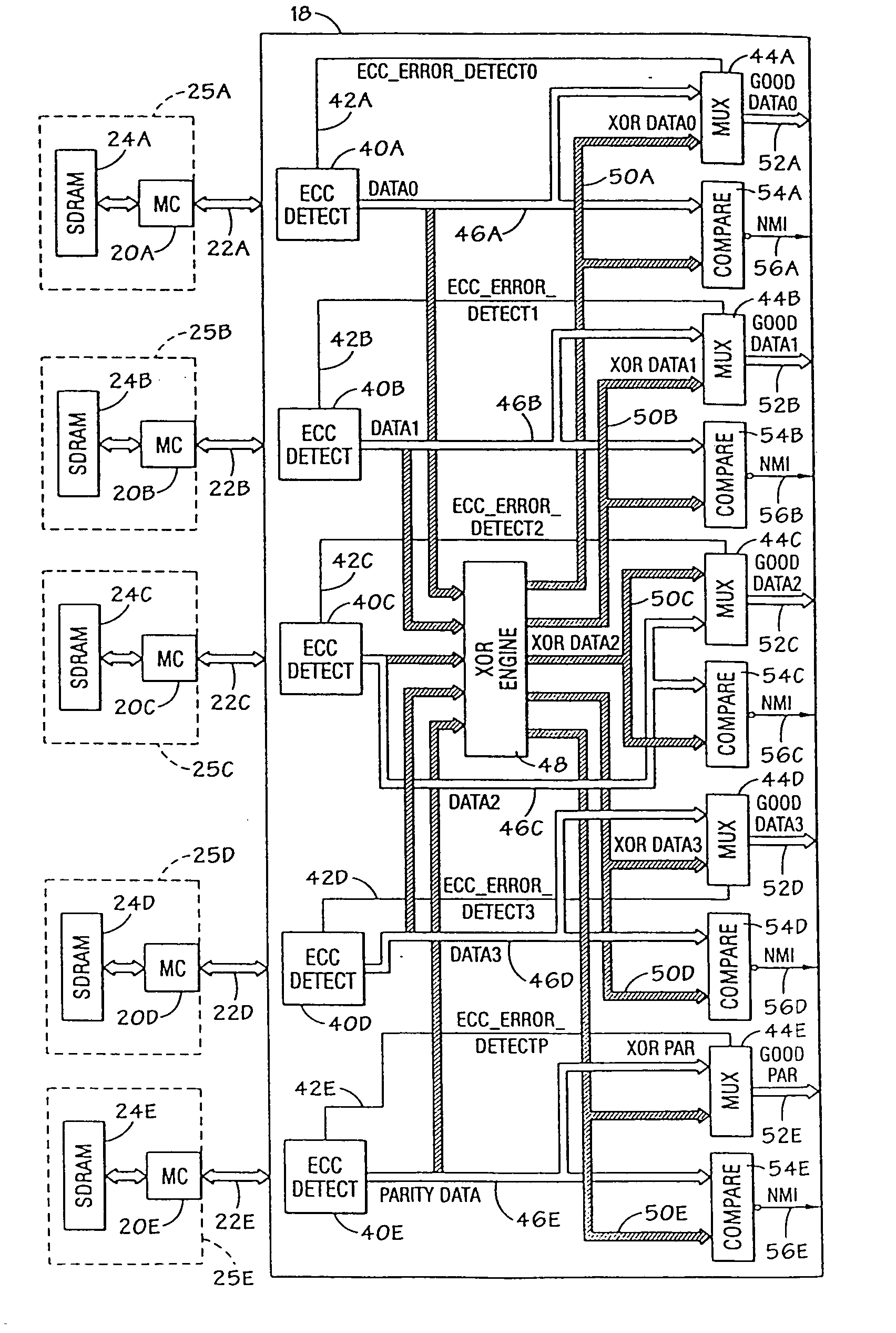
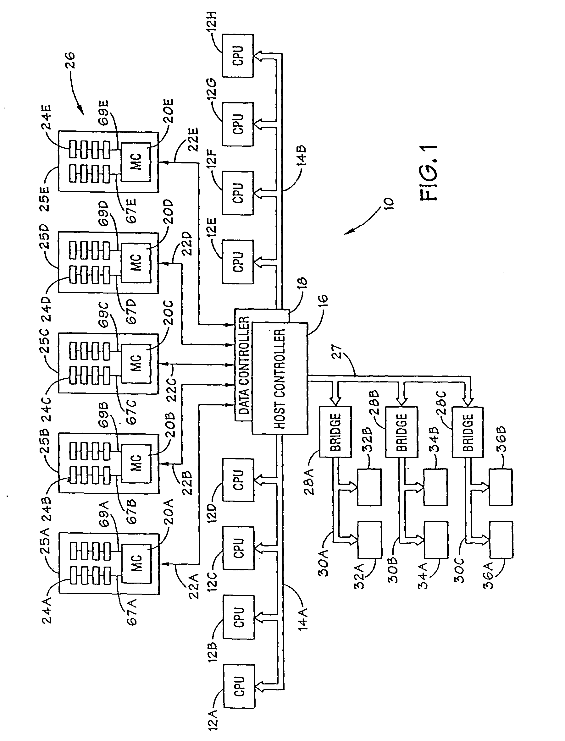
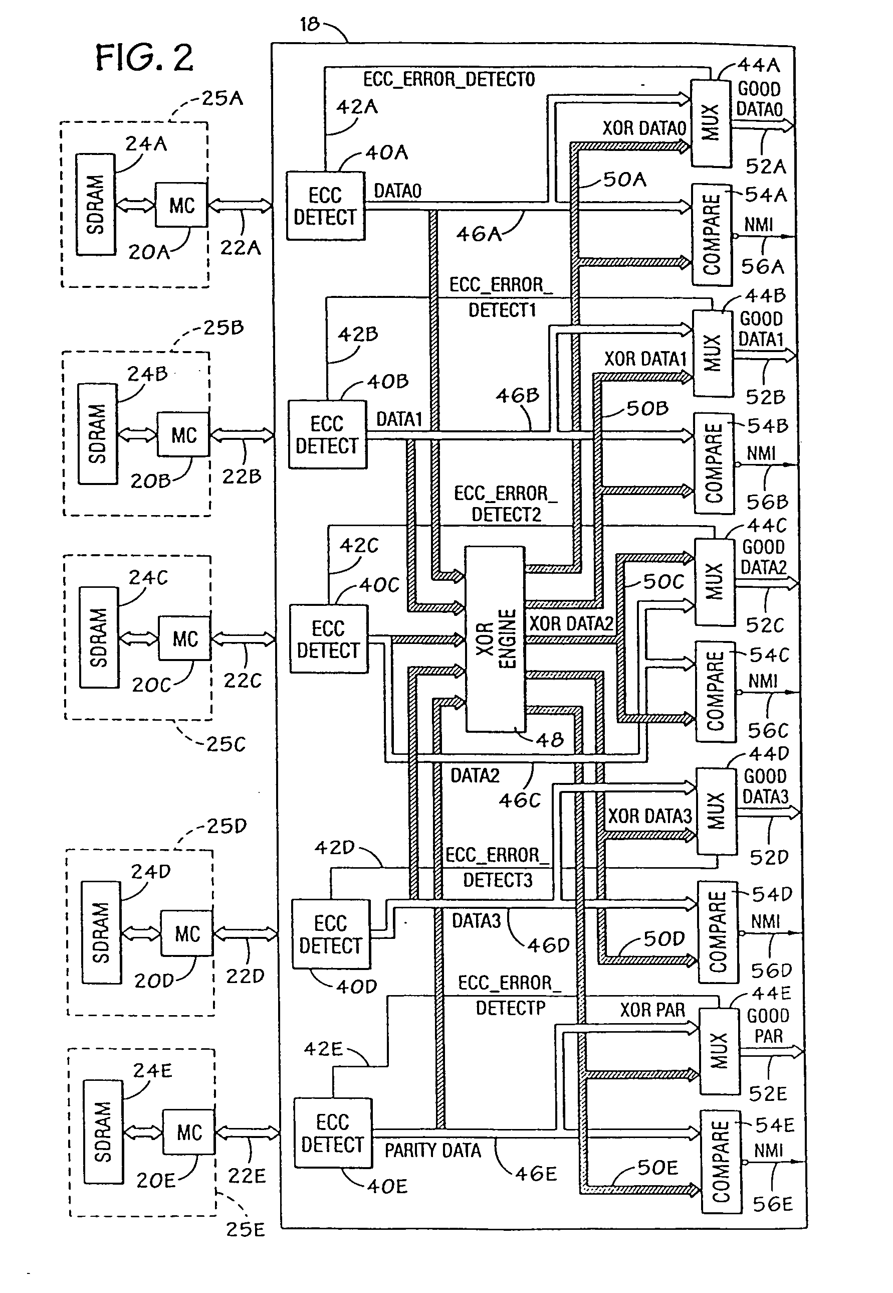
[0022] Turning now to the drawings and referring initially to FIG. 1, a block diagram of an exemplary computer system with multiple processor buses and a...


PUM


Abstract

A computer system includes a plurality of memory modules that contain semiconductor memory, such as DIMMs. The system includes a host / data controller that utilizes an XOR engine to store data and parity information in a striped fashion on the plurality of memory modules to create a redundant array of industry standard DIMMs (RAID). The host / data controller also interleaves data on a plurality of channels associated with each of the plurality of memory modules. To optimize memory bandwidth and reduce memory latency, various techniques are implemented in the present RAID system. Present techniques include providing dual memory arbiters, sorting read cycles by chip select or bank address, providing programmable upper and lower boundary registers to facilitate programmable memory mapping, and striping and interleaving memory data to provide a burst length of one.

Description

[0001] 1. Field Of The Invention[0002] This invention relates generally to memory systems and, more particularly, to redundant memory systems with reduced memory latency and bandwidth optimization.[0003] 2. Background Of The Related Art[0004] This section is intended to introduce the reader to various aspects of art which may be related to various aspects of the present invention which are described and / or claimed below. This discussion is believed to be helpful in providing the reader with background information to facilitate a better understanding of the various aspects of the present invention. Accordingly, it should be understood that these statements are to be read in this light, and not as admissions of prior art.[0005] Computer usage has increased dramatically over the past few decades. In the past, computers were relatively few in number and primarily used as scientific tools. However, with the advent of standardized architectures and operating systems, computers have become...

Claims


Application Information

Patent Timeline
Patent Type & Authority Applications(United States)
IPC IPC(8): G06F13/16
CPCG06F13/1642
Inventor JOHNSON, JEROME J.CLARK, BENJAMIN H.PICCIRILLO, GARY J.MACLAREN, JOHN M.
Owner HEWLETT PACKARD DEV CO LP
Why Eureka
Try Eureka