

Semiconductor device, stacked semiconductor device, methods of manufacturing the same, circuit board, and electronic instrument
a semiconductor and semiconductor technology, applied in the direction of semiconductor devices, semiconductor/solid-state device details, electrical apparatus, etc., can solve the problems of increasing the cost of additional steps and extremely limited space for mounting electronic parts
- Summary
- Abstract
- Description
- Claims
- Application Information
AI Technical Summary
Benefits of technology
Problems solved by technology
Method used
Image

Examples
Embodiment Construction
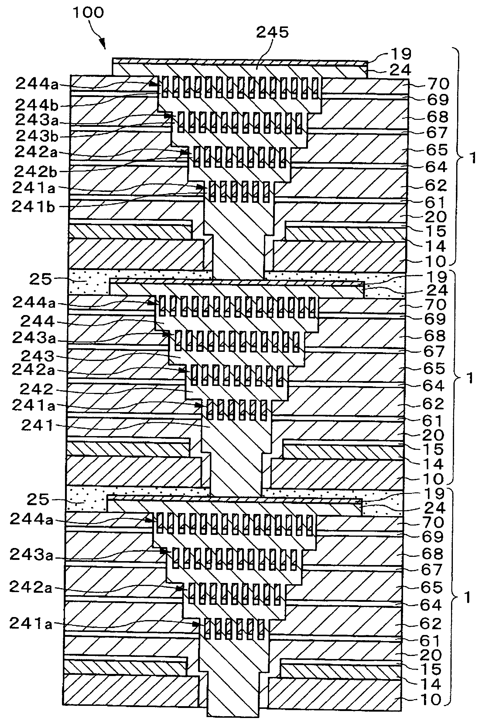
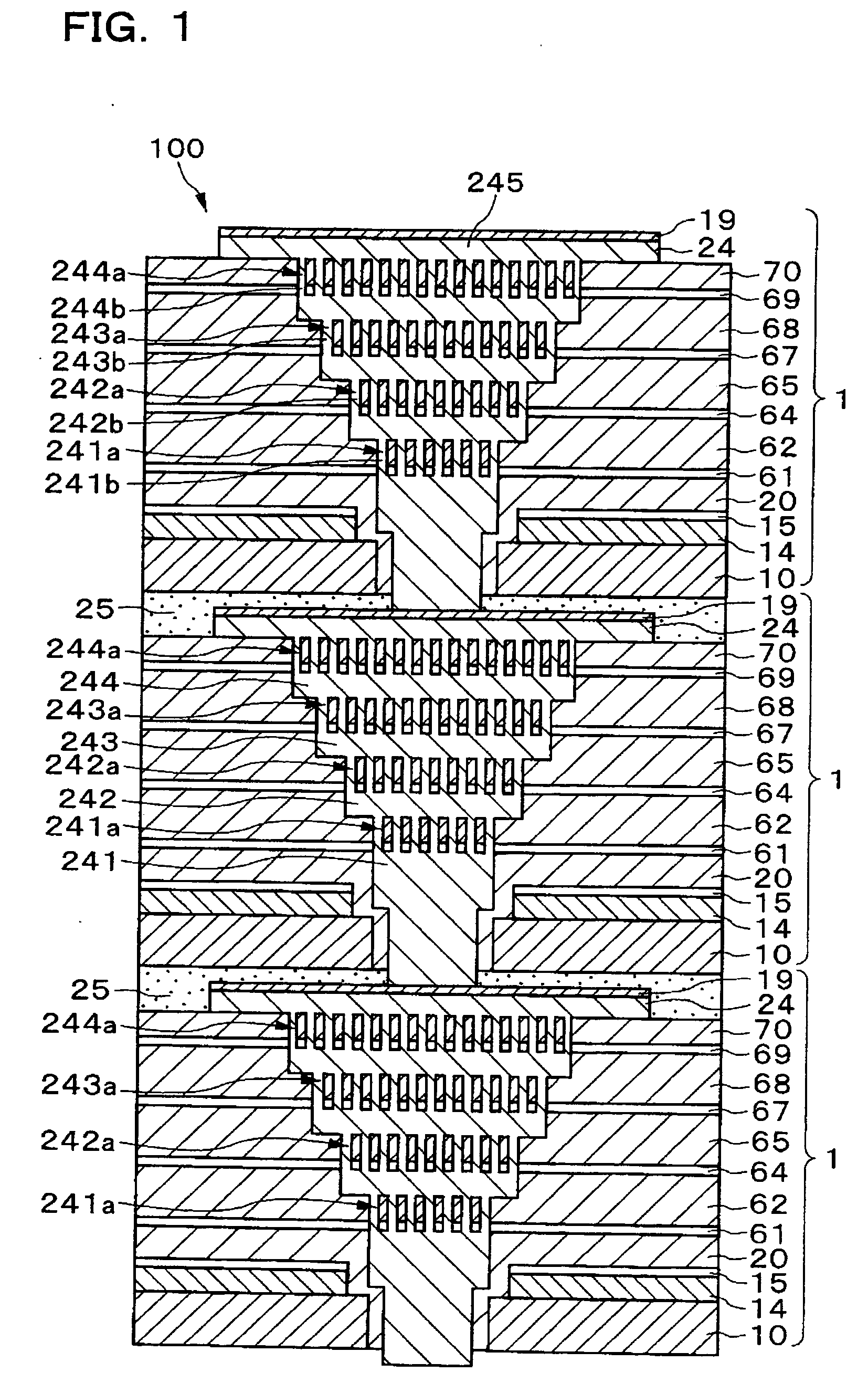
[0045] Embodiments of the present invention are achieved in view of the above-described problems, and may provide a method of manufacturing a semiconductor device which enables the manufacturing cost to be reduced by simplifying formation steps of a conductive material.
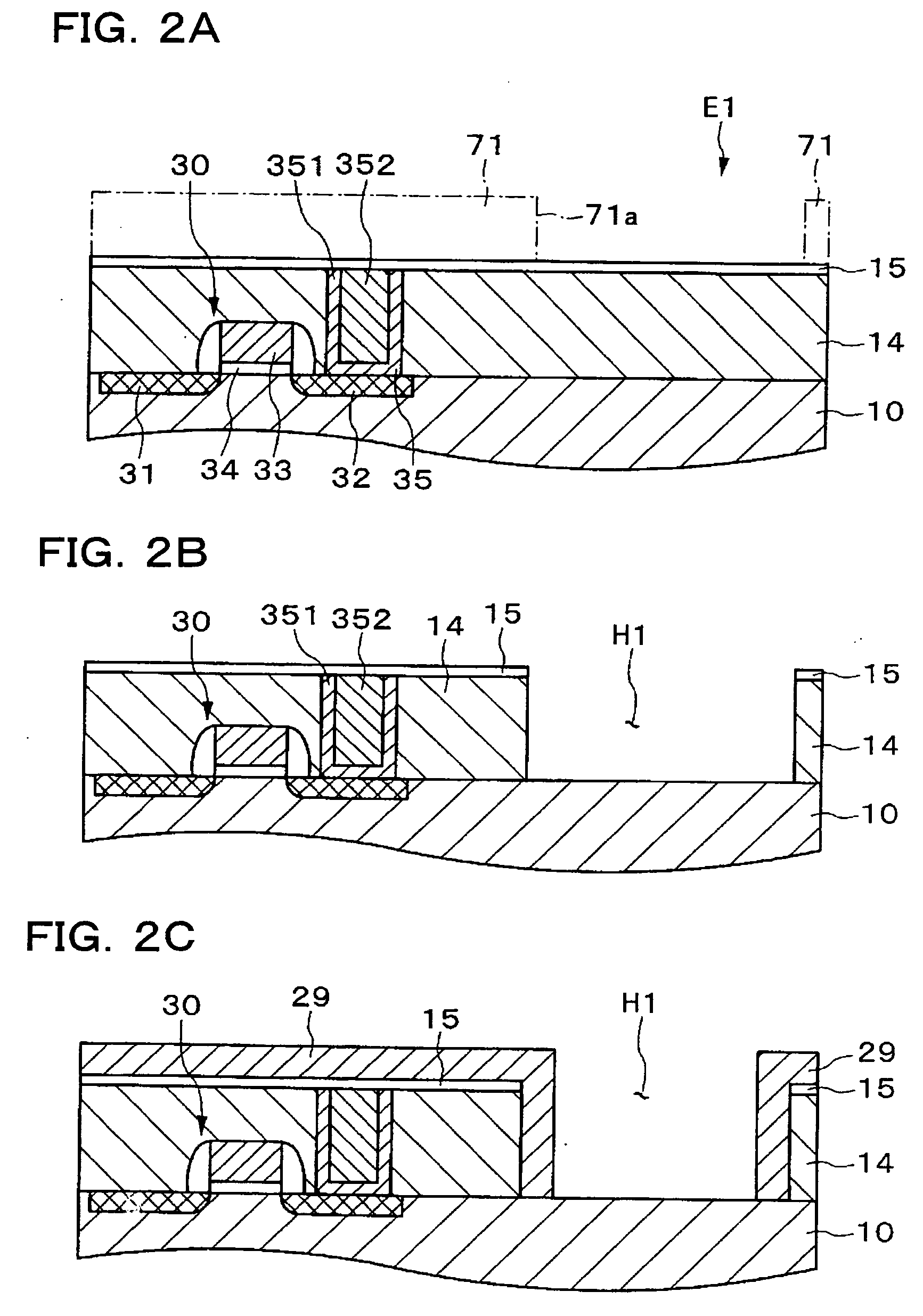
[0046] According to one embodiment of the present invention, there is provided a method of manufacturing a semiconductor device having a connection terminal and a substrate on which a circuit section and an electrode are stacked in this order, the circuit section having a multilayer interconnect structure, the electrode being conductively connected to the circuit section, and the connection terminal penetrating the substrate and being conductively connected to the electrode, the method comprising: [0047] an insulating film formation step of forming an insulating film on the substrate; [0048] a hole formation step of forming a plurality of connection holes in the insulating film at a position corresponding to a connec...
PUM
 Abstract
Description
Claims
Application Information