Deposition mask, method for manufacturing display unit using it, and display unit

a technology of display unit and mask, which is applied in the manufacture of electrode systems, electric discharge tubes/lamps, discharge tubes luminescent screens, etc., can solve the problems of lowering the aperture ratio, reduce the wiring resistance difference between the power source and respective organic light emitting devices, and improve the aperture ratio of the display unit

Active Publication Date: 2005-01-06
SONY CORP
View PDF3 Cites 122 Cited by
  • Summary
  • Abstract
  • Description
  • Claims
  • Application Information

AI Technical Summary

Benefits of technology

[0020] In the display unit according to an embodiment of the present invention, the stripe-shaped continuous organic layer is provided over at least two lines of the matrix configuration of the number of organic light emitting elements in common. Therefore, a film thickness distribution is decreased in the extensional direction of the continuous organic layer. Further, the notch parts are provided on the side wall part of the continuous organic layer corresponding to the area between lines of the number of first electrodes, and the auxiliary electrode and the second electrode are electrically connected through the contact part formed at these notch parts. Therefore, a wiring resistance difference between the power source and respective organic light emitting devices is reduced.
[0021] In an embodiment, the present invention provides a deposition mask which can improve an aperture ratio of a display unit, a method for manufacturing a display unit using it, and a display unit. A red continuous organic layer, a green continuous organic layer, and a blue continuous organic layer are provided over two or more lines of a matrix configuration of organic light emitting devices in common. Differently from the conventional case wherein the organic layer is formed corresponding to each organic light emitting device, a film thickness distribution in the extensional direction of the red continuous organic layer, the green continuous organic layer, and the blue continuous organic layer is dissolved, and an aperture ratio can be improved by just that much. Notch parts are provided for the red continuous organic layer, the green continuous organic layer, and the blue continuous organic layer. At these notch parts, a contact part between a second electrode and an auxiliary electrode is formed. Therefore, voltage drop of the second electrode can be effectively inhibited.

Problems solved by technology

Therefore, there has been a problem that when using the conventional deposition mask 140, the effective light emitting region 117A is limited, so that an aperture ratio is lowered.

Method used


Image

  • Deposition mask, method for manufacturing display unit using it, and display unit
  • Deposition mask, method for manufacturing display unit using it, and display unit
  • Deposition mask, method for manufacturing display unit using it, and display unit

Examples


Embodiment Construction

[0058] The present invention relates to a deposition mask, a method for manufacturing a display unit using same, and a display unit. More specifically the present invention relates to a deposition mask suitable for manufacturing a display unit using organic light emitting devices, a method for manufacturing a display unit using same, and a display unit.

[0059] An embodiment of the present invention will be described in detail hereinbelow with reference to the drawings.

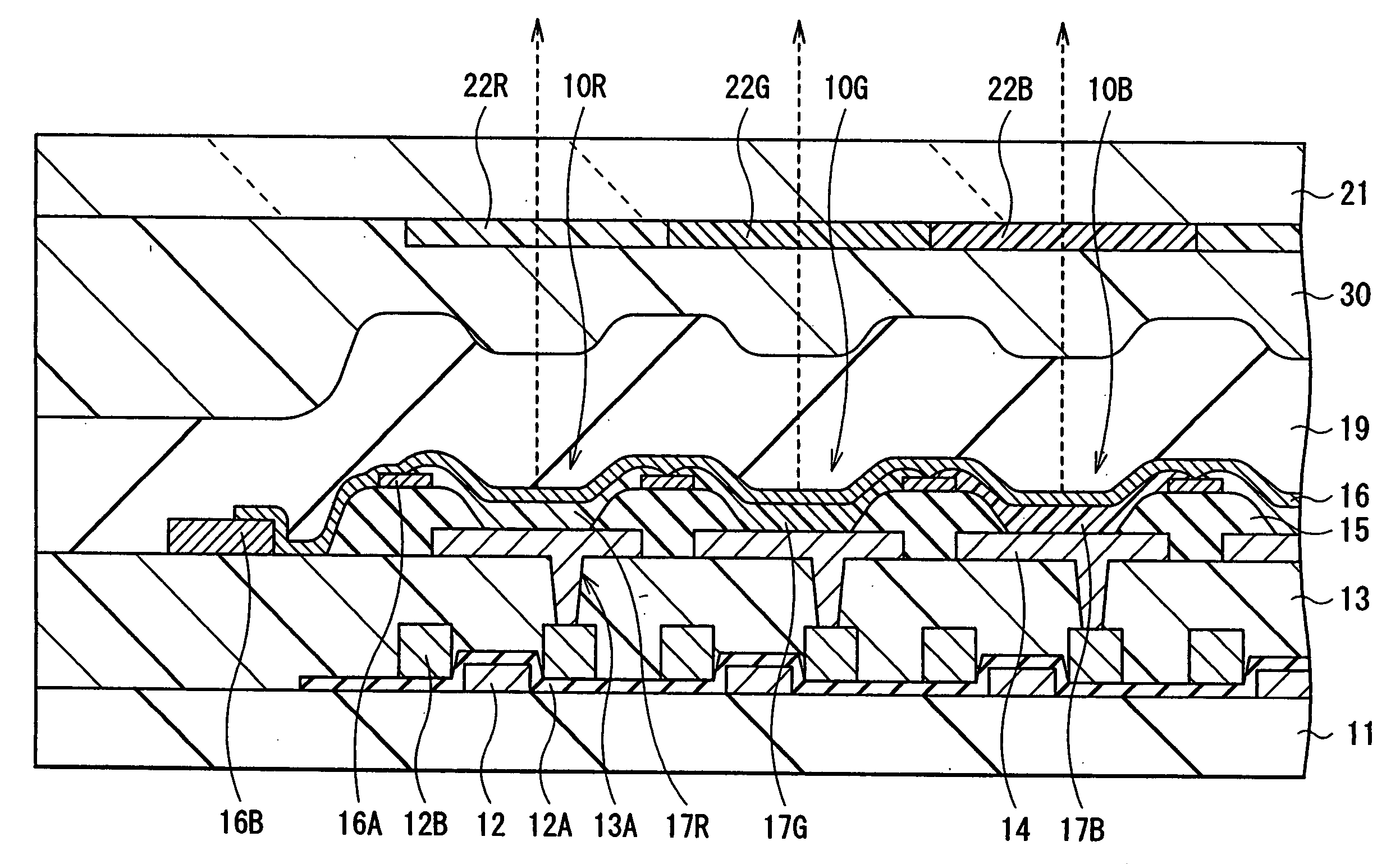
[0060] With reference to FIGS. 9 to 31B, a method for manufacturing a display unit according to an embodiment of the invention and a deposition mask used for the display unit will be described. This display unit is used, for example, as an ultra thin organic light emitting display. As shown in FIG. 9, many pixels are arranged in the shape of a matrix as a whole by constructing a matrix configuration constructed by a number of lines and columns of organic light emitting devices 10R, 10G, and 10B on a substrate 11, sett...


PUM

PropertyMeasurementUnit
thicknessaaaaaaaaaa
thicknessaaaaaaaaaa
vol %aaaaaaaaaa

Abstract

A deposition mask and a display unit and method of manufacturing same are provided. A red continuous organic layer, a green continuous organic layer, and a blue continuous organic layer are provided over two or more lines of a matrix configuration of organic light emitting devices in common. A film thickness distribution in the extensional direction of the red, green and blue continuous organic layer is dissolved, and an aperture ratio can be improved by just that much.

Description

CROSS REFERENCES TO RELATED APPLICATIONS [0001] This application claims priority to Japanese Patent Application No. P2003-132791, filed on May 12, 2003, the disclosure of which is herein incorporated by reference. BACKGROUND OF THE INVENTION [0002] The present invention relates to a deposition mask, a method for manufacturing a display unit using same, and a display unit. More specifically the present invention relates to a deposition mask suitable for manufacturing a display unit using organic light emitting devices, a method for manufacturing a display unit using same, and a display unit. [0003] In recent years, as a display unit instead of a liquid crystal display, an organic light emitting display which uses organic light emitting devices has been used. The organic light emitting display has characteristics that its viewing angle is wide and its power consumption is low since it is a self-luminous type display. The organic light emitting display is also thought of as a display h...

Claims


Application Information

Patent Timeline
Patent Type & Authority Applications(United States)
IPC IPC(8): H05B33/10C23C14/04H01L27/32H01L51/00H01L51/30H01L51/40H01L51/50H01L51/52H01L51/56H05B33/04H05B33/06
CPCC23C14/042H01L27/3211H01L27/3244H01L51/0008H01L51/005H01L51/0059H01L51/5262H01L51/0081H01L51/5203H01L51/56H01L2251/5315H01L51/0012H01L27/32H01L51/0062H10K59/35H10K59/12H10K59/131H10K71/16H10K85/111H10K85/60H10K85/631H10K85/649H10K85/324H10K50/82H10K50/844H10K71/00H10K2102/00H10K2102/3026H10K2102/351H10K59/805H05B33/10H10K71/166H10K50/81H10K50/85H10K50/805H10K50/814H10K50/824H10K59/00H10K71/191H10K50/11H10K59/1201
Inventor YAMAGUCHI, MASARU
Owner SONY CORP
Why Eureka
Try Eureka