

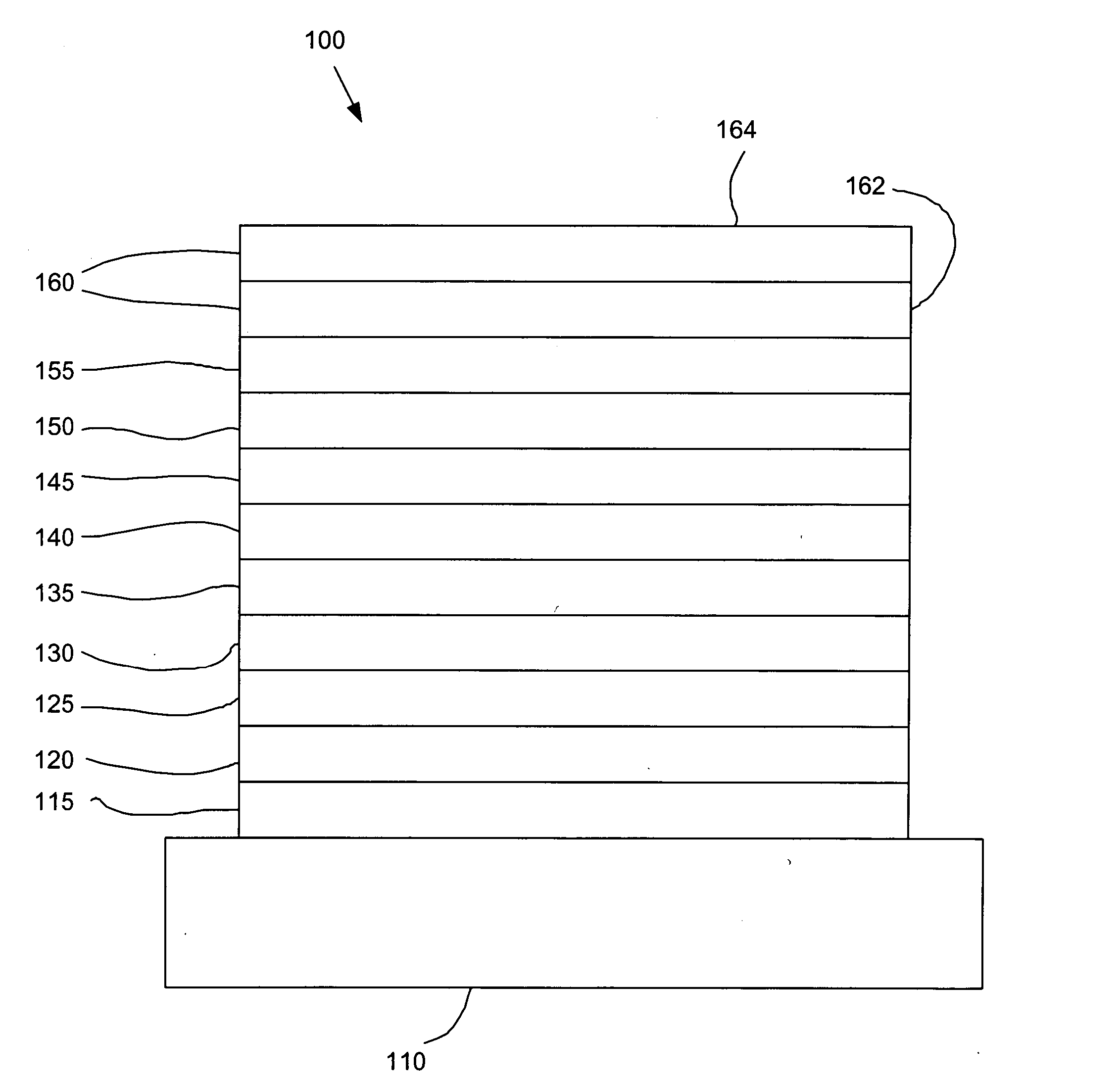
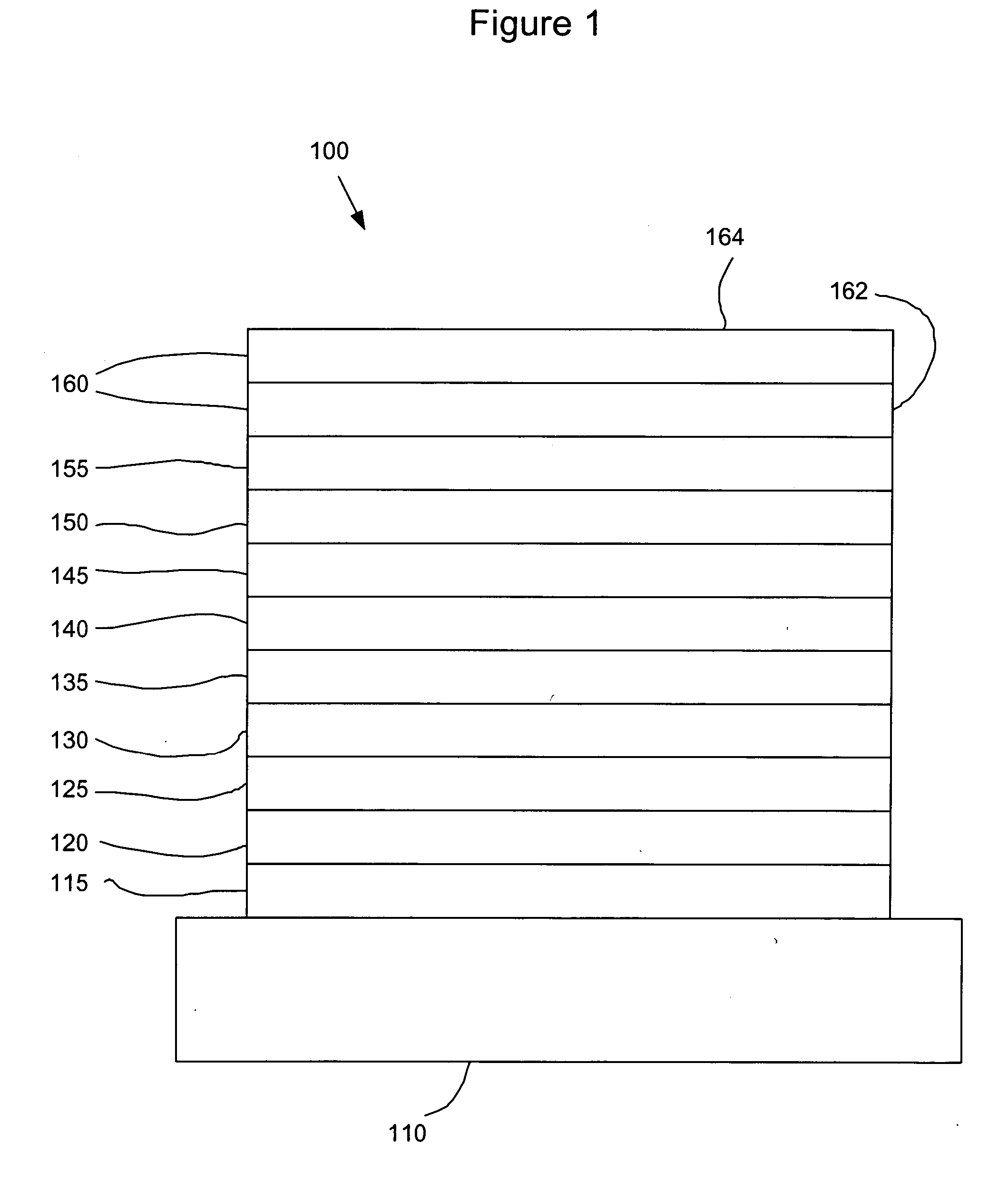
Organic light emitting device structures for obtaining chromaticity stability
a light-emitting device and organic technology, applied in the direction of solid-state devices, semiconductor devices, thermoelectric devices, etc., can solve the problems of low efficiency, complicated design of such devices, and devices that suffer, and achieve high color stability
- Summary
- Abstract
- Description
- Claims
- Application Information
AI Technical Summary
Benefits of technology
Problems solved by technology
Method used
Image

Examples
example 1
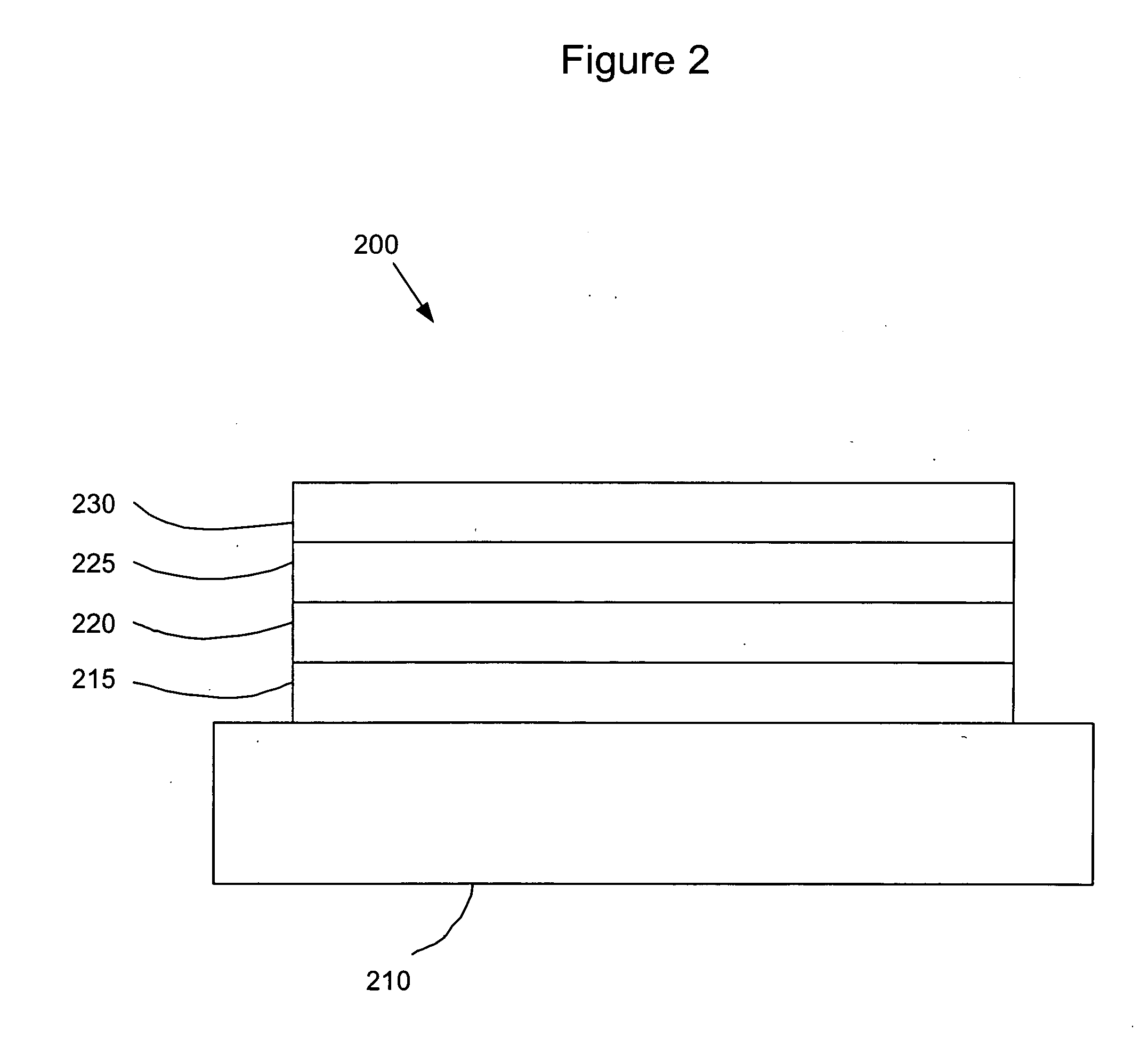
An OLED was prepared with the structure ITO / CuPc(100 Å)INPD(300 Å) / CBP:Irppy(50 Å, 6%) / mCP:Ir(F2CNppy)2(pic)(200 Å,6%) / CBP:Ir(pq)2(acac)(50 Å,6%) / BAlq(400 Å) / LiF(5 Å) / Al(100 Å). FIG. 4 shows the plots of the normalized emission spectra at various current densities for this device. FIG. 5 shows the plots of luminous efficiency and power efficiency vs. luminance for this device.
example 2
An OLED was prepared with the structure ITO / CuPc(100 Å) / NPD(300 Å) / mCP:Ir(F2CNppy)2(pic)(200 Å, 6%) / CBP:Ir(pq)2(acac)(50 Å,6%) / CBP:Irppy (50 Å,6%) / Balq(400 Å) / LiF(5 Å) / Al(1000 Å). FIG. 6 shows the plots of the normalized emission spectra at various current densities for this device. FIG. 7 shows the plots of luminous efficiency and power efficiency vs. luminance for this device.
example 3
An OLED was prepared with the structure ITO / CuPc(100 Å) / NPD(300 Å) / mCP:Irppy(6%,50 Å) / mCP:Ir(F2CNppy)2(pic)(6%,225 Å) / CBP:Ir(pq)2(acac)(6%,25 Å) / BAlq(400 Å) / LiF(5 Å) / Al(1000 Å). FIG. 8 shows the plots of the normalized emission spectra at various current densities for this device. FIG. 9 shows the plots of luminous efficiency and power efficiency vs. luminance for this device.
PUM
 Abstract
Description
Claims
Application Information