Modulation circuit device, modulation method and radio communication device

a modulation circuit and radio communication technology, applied in modulation, pulse technique, digital transmission, etc., can solve the problems of large amount of memory required, complicated control of these transistors, and distortion of signals outputted from amplitude modulators

Active Publication Date: 2005-01-13
PANASONIC CORP
View PDF14 Cites 120 Cited by
  • Summary
  • Abstract
  • Description
  • Claims
  • Application Information

AI Technical Summary

Benefits of technology

[0096] (1) from among the magnitude of said amplitude signals to be inputted, said waveform shaping step makes said intersecting point round and shaped so that the first order differential coefficient and the second order differential coefficient involved with the magnitude of said amplitude signals to be inputted of the magnitude of said signal from the output of said waveform shaping means corresponding to the portion made round and shaped of the side related to said first prescribed value does not become negative, respectively, and / or wherein (2), from the magnitude of among said amplitude signals to be inputted, said waveform shaping means makes said intersecting point round and shaped, so that the first order differential coefficient involved with the magnitude of said amplitude signals to be inputted of the magnitude of said signal of the output of said waveform shaping means corresponding to the portion to be made round and shaped related to said second prescribed value does not become negative and the second order differential coefficient does not become positive.

Problems solved by technology

However, when the dynamic range is enlarged, the second power of the supply voltage is forced out from the range of the linear region of FIG. 9(a) and the flat region of FIG. 9(b), and the signal outputted from the amplitude modulator ends up being distorted.
This is difficult to realize by a single transistor, and moreover, in the case where this is realized by using a plurality of transistors, it becomes complicated to control these transistors, and moreover, in the case where distortion correction is performed by a table, the amount of memory required becomes large.
That is, in the case where the transistor used in the amplitude modulator of the modulator for performing the conventional polar modulation is a transistor not having the linearity in a wide range, there is a problem in that a signal sufficiently deeply amplitude-modulated cannot be obtained.
This is difficult to realize by a single transistor, and moreover, in the case where this is realized by using a plurality of transistors, it becomes complicated to control these transistors, and moreover, in the case where distortion correction is performed by a table, there is a problem in that the amount of memory required becomes large.

Method used


Image

  • Modulation circuit device, modulation method and radio communication device
  • Modulation circuit device, modulation method and radio communication device
  • Modulation circuit device, modulation method and radio communication device

Examples


first embodiment

[0166] First, the first embodiment will be described.

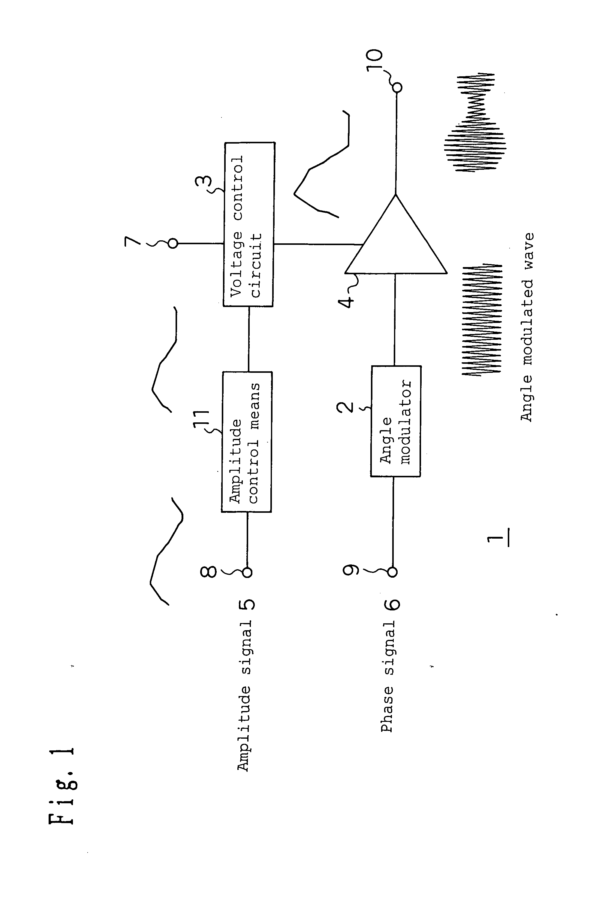
[0167]FIG. 1 shows a modulation circuit device 1 of the first embodiment.

[0168] The modulation circuit device 1 of the first embodiment is, similarly to the conventional art, is used for a transmitting circuit device used for the terminal of a mobile phone and a base station.

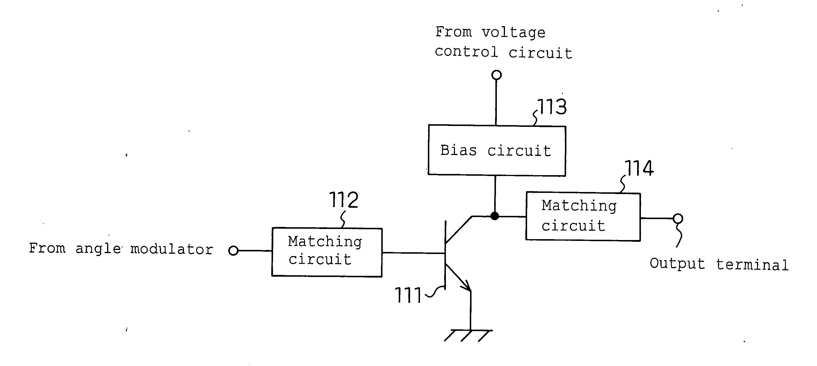
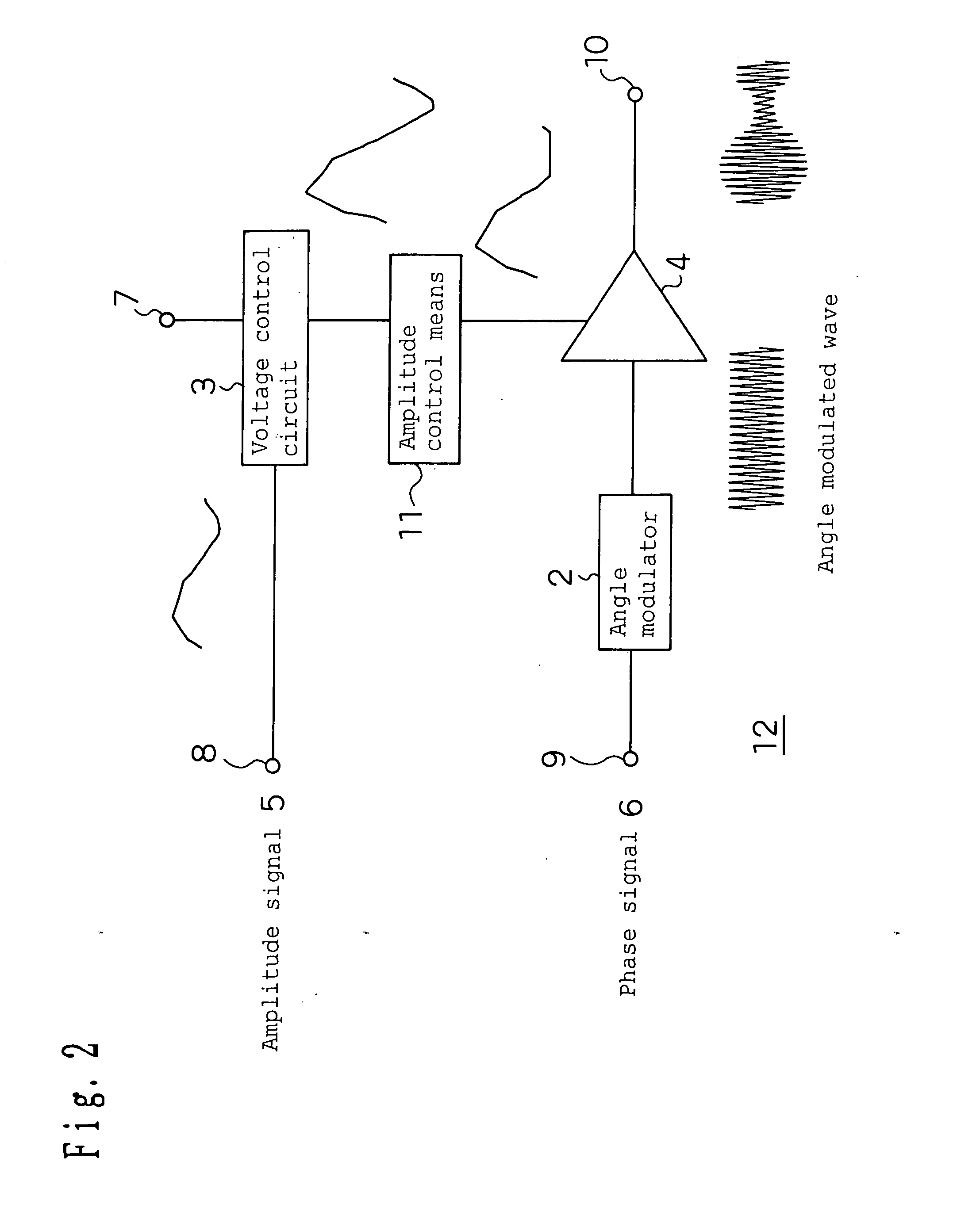
[0169] The modulation circuit device 1 consists of an angle modulator 2, a voltage control device 3, an amplitude modulator 4, and amplitude control means 11.

[0170] The angle modulator 2 is a circuit to angle-modulate a carrier wave by a phase signal 6 inputted from a second input terminal 9.

[0171] The voltage control circuit 3 is used to supply a stable voltage to the amplitude modulator 4, and is a circuit to generate an output signal based on the signal of the output from the amplitude control means 11.

[0172] As the voltage control circuit 3, a series regulator as shown in FIG. 7 can be used. In FIG. 7, a comparator 121 is a circuit to compare the inp...

second embodiment

[0209] Next, a second embodiment will be described.

[0210] In FIG. 3 is shown a constitution of a modulation circuit device 18 of the second embodiment. The modulation circuit device 18 of the second embodiment is used for a radio communication device, which has a function to control a transmission power according to the distance between the base station of a mobile phone and a terminal.

[0211] The modulation circuit device 18 of the second embodiment is, similarly to a conventional art, is used for a transmission circuit device used in the terminal of a mobile phone and a base station. Particularly, the modulation circuit device 18 of the second embodiment is suitable for a transmitter having a power control function.

[0212] That is, the modulation circuit device 18 consists of an angle modulator 2, amplitude control means 11, a first amplitude modulator 13, a second amplitude modulator 14, a switch 15, a first voltage control circuit 16, and a second voltage control circuit 17.

[0...

third embodiment

[0242] Next, a third embodiment will be described.

[0243] The amplitude control means 11 of the first embodiment as described by using FIG. 1 shapes the waveform of the amplitude signal 5 so that the voltage of the amplitude signal 5 of a portion which becomes small becomes a threshed value when the voltage of the amplitude signal 5 inputted from the first input terminal 8 becomes lower than the threshold value. For example, when the signal shown in FIG. 10(a) is inputted to the amplitude control means 11 as the amplitude signal 5, as a result of performing the waveform shaping at the amplitude control means 11, the signal shown in FIG. 10(b) is outputted from the voltage control circuit.

[0244] As evident from FIG. 10(b), with regard to the waveform of the signal outputted from the amplitude control means 11 of the first embodiment, the intersecting point with the signal which is cut and shaped by the threshold value and the signal which is not cut nor shaped by the threshold value...


PUM


Abstract

The amplitude modulator comprises: an angle modulator for angle-modulating a phase signal to be inputted; a waveform shaping means in which, (1) when the magnitude of an amplitude signal to be inputted becomes smaller than a first prescribed value, a waveform of the amplitude signal is shaped so that the magnitude of the amplitude signal of the portion which becomes small becomes the first prescribed value; and/ or (2) the waveform shaping means in which, when the magnitude of the amplitude signal to be inputted becomes larger than the second prescribed value which is larger than the first prescribed value, the waveform of the amplitude signal is shaped so that the magnitude of the amplitude signal of the portion which becomes larger becomes the second prescribed value; and an amplitude modulator for amplitude modulating the signal of the output of the angle modulator by the signal of the output of the waveform shaping means.

Description

BACKGROUND OF THE INVENTION [0001] 1. Field of the Invention [0002] The present invention relates to a modulation circuit device used for a transmission circuit device such as a mobile phone and the like, and more in particular, it relates to a modulation circuit device for polar-modulating an input signal, a modulation method and a radio communication device using the same. [0003] 2. Related Art of the Invention [0004] A quadrature modulator has been widely used for a modulation circuit device used for a transmission circuit device, which is used for the terminal of a mobile phone and a base station. In recent years, however, a polar modulation has been highlighted, which is a modulation form allowing data to be carried by a polar coordinate system (phase and amplitude) (for example, Japanese Patent Laid-Open No. 09-18451). The disclosure of Japanese Patent Laid-Open No. 09-18451 is incorporated herein by reference in its entirety. [0005] In FIG. 31 is shown a conventional modulati...

Claims


Application Information

Patent Timeline
Patent Type & Authority Applications(United States)
IPC IPC(8): H03C5/00H03F1/02H03K7/06H04L27/36
CPCH03C5/00H03F1/0222H03F1/025H04L27/361H03F2200/372H03F2203/7239H03F1/0277
Inventor MATSUURA, TORUADACHI, HISASHIUDAGAWA, MASAHARU
Owner PANASONIC CORP
Why Eureka
Try Eureka