Gate length proximity corrected device

a technology of proximity correction and gate length, which is applied in the field of semiconductor devices, can solve the problems of creating timing skews in circuits, devices with very narrow gate widths, and being more susceptible to photolithographic proximity effects

Inactive Publication Date: 2005-01-13
QIMONDA +1
View PDF12 Cites 176 Cited by
  • Summary
  • Abstract
  • Description
  • Claims
  • Application Information

AI Technical Summary

Benefits of technology

[0005] A third aspect of the present invention is a method of designing a device having a gate length and a gate width comprising: providing a design grid of gate shapes, each gate shape having a fixed width defined by opposite ends and extending in a widthwise direction, a useable fixed width less than the fixed width and a fixed length extending in a lengthwise direction, the lengthwise direction substantially perpendicular to the widthwise direction, the gate shapes arranged substantially parallel to each other in the widthwise direction and periodically spaced apart a fixed distance in the lengthwise direction; and forming a functional gate shape from one or more of the gate shapes.

Problems solved by technology

Devices with very narrow gate widths are much more susceptible to photolithographic induced proximity effects.
Proximity effects are especially worrisome when many gates of different length and width occur in physical proximity because devices expected to have the same speeds could have different gate lengths and widths (hence different speeds), creating timing skews in circuits made from these devices.

Method used


Image

  • Gate length proximity corrected device
  • Gate length proximity corrected device
  • Gate length proximity corrected device

Examples


first embodiment

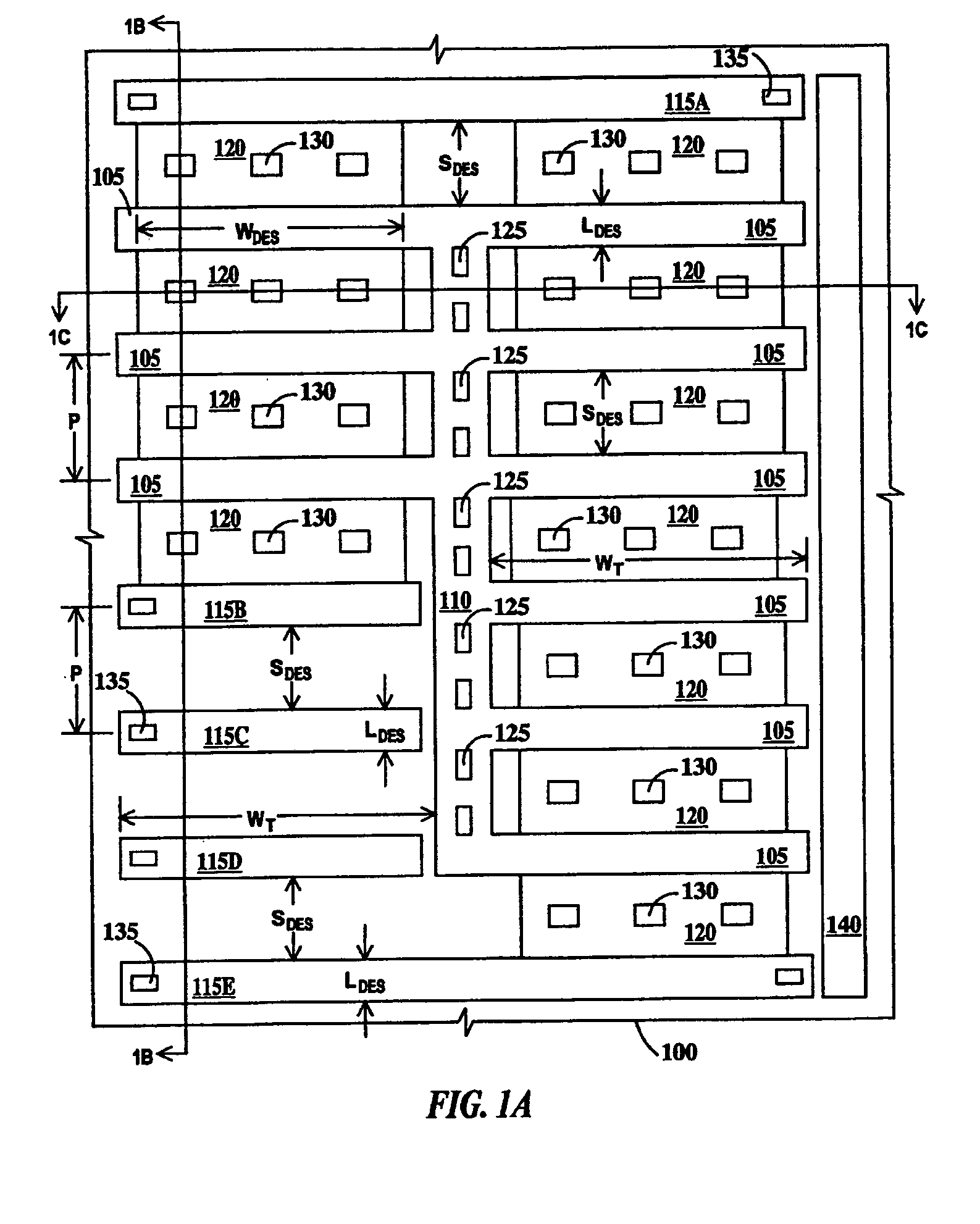
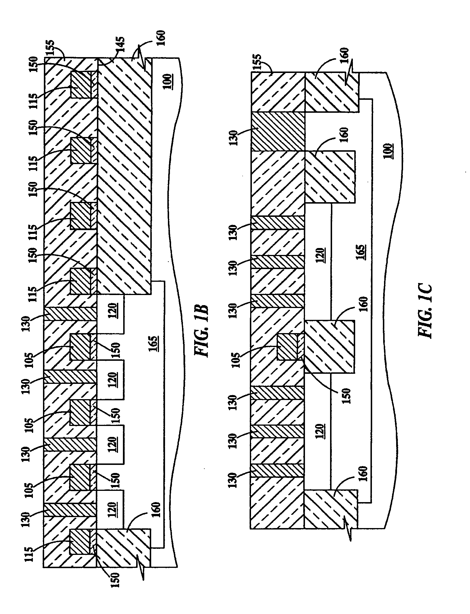
[0017]FIG. 1A is top view of a device according to the present invention. In FIG. 1A, formed on a semiconductor substrate 100, such as a bulk silicon or silicon-on-insulator (SOI) substrate, are a multiplicity of parallel functional gate conductors 105 integral to and extending perpendicular from a spine 110 and a multiplicity of dummy gate conductors 115A through 115E. Dummy gate conductors 115A through 115E are arranged parallel to functional gate conductors 105. Each functional gate conductor 105 extends a distance WT from spine 110. Functional gate conductors 105 and dummy gate conductor 115A through 115E are spaced apart from immediately adjacent to functional gate conductors or immediately adjacent to dummy gate conductors a distance SDES and have a width LDES. In one example, SDES and LDES are the minimum design groundrule distances. A pitch P=SDES+LDES may therefore be defined. The edges (or centers) of both functional gate conductors 105 and dummy gate conductor 115A throug...

second embodiment

[0029]FIG. 3 is top view of a pair of devices according to the present invention. FIG. 3 illustrates an NFET 195A and a PFET 195B formed adjacent to one another as would be used in forming the FETs of an inverter circuit.

[0030] In FIG. 3, formed on a semiconductor substrate 200, are a multiplicity of parallel functional gate conductors 205A and 205B integral to and extending perpendicular from spines 210A and 210B respectively and a multiplicity of dummy gate conductors 215A and 215B. Dummy gate conductors 215A and 215B are arranged parallel to respective functional gate conductors 205A and 205B. Functional gate conductors 205A and 205B and dummy gate conductor 215A and 215B are spaced apart from immediately adjacent functional gate conductors or immediately adjacent dummy gate conductors a distance SDES and have a width WDES and a channel length LDES. Pitch P SDES+LDES is therefore the same as defined supra. Both functional gate conductors 205A and 205B and dummy gate conductor 215...

third embodiment

[0034]FIG. 4 is top view of a pair of devices according to the present invention. FIG. 4 illustrates an NFET 295A and a PFET 295B formed adjacent to one another as would be used in forming the FETs of an inverter circuit. NFET 295A and PFET 295B are less wide than NFET 195A and PFET 195B of FIG. 3.

[0035] In FIG. 4, formed on a semiconductor substrate 300, is a multiplicity of parallel functional gate conductors 305A and 305B integral to and extends perpendicular from spines 310A and 310B respectively, and a multiplicity of dummy gate conductors 315A1, 315A2 and 315B1 and 315B2. Dummy gate conductors 315A1 and 315B1 are arranged parallel to respective functional gate conductors 305A and 305B. Dummy gate conductors 315A2 and 315B2 are arranged in line with respective functional gate conductors 305A and 305B. Functional gate conductors 305A and 305B and dummy gate conductor 315A1 and 315B1 are spaced apart from immediately adjacent functional gate conductors or immediately adjacent dum...


PUM


Abstract

An electronic device including: a semiconductor substrate having an array of gate conductors, each having a length and a width, comprised of dummy gate conductors and functional gate conductors extending in a widthwise direction, the gate conductors positioned substantially parallel to each other in the widthwise direction and periodically spaced apart a fixed distance in a direction substantially perpendicular to the widthwise direction.

Description

BACKGROUND OF INVENTION [0001] The present invention relates to the field of semiconductor devices; more specifically, it relates to a gate structure corrected for gate length proximity effects and the method of designing and fabricating the corrected gate structure. [0002] As device sizes decrease gate lengths of devices decrease as well. Devices with very narrow gate widths are much more susceptible to photolithographic induced proximity effects. Proximity effects cause a printed gate to deviate from a nominal or designed gate length and width (or shape). Proximity effects are especially worrisome when many gates of different length and width occur in physical proximity because devices expected to have the same speeds could have different gate lengths and widths (hence different speeds), creating timing skews in circuits made from these devices. SUMMARY OF INVENTION [0003] A first aspect of the present invention is an electronic device comprising: a semiconductor substrate having ...

Claims


Application Information

Patent Timeline
Patent Type & Authority Applications(United States)
IPC IPC(8): H01L29/423G06F17/50H01L21/3205H01L21/82H01L21/822H01L21/8234H01L21/8238H01L23/52H01L27/02H01L27/04H01L27/088H01L27/092H01L27/12H01L29/49
CPCG06F17/5068H01L21/823437H01L27/0207H01L27/1203H01L2924/0002H01L2924/00G06F30/39
Inventor BUTT, SHAHIDELLIS, WAYNE F.GABRIC, JOHN A.
Owner QIMONDA
Why Eureka
Try Eureka