Method for forming a bond pad interface

Inactive Publication Date: 2005-01-20
NXP USA INC
View PDF19 Cites 36 Cited by
  • Summary
  • Abstract
  • Description
  • Claims
  • Application Information

AI Technical Summary

Problems solved by technology

However, copper is a non-self-passivating metal, and oxidation or corrosion of copper bond pads can occur when the die is exposed to the atmosphere or a non-hermitic package allows moisture to interact with the copper bond pad.
This corrosion can degrade the ability to bond leads or bumps to the bond pads and can also cause the bond to decay and fail over time.
Problems can arise in composite bond pad structures when test and probe operations are performed.
As such, the physical contact by such elements can damage the interface between the different metals comprising the composite bond pad structure.
The damage produced can result in the formation of intermetallics at the copper-aluminum interface if the barrier is broken between the underlying copper layer and the aluminum capping layer.
The aluminum-copper intermetallic can have undesirable characteristics including reduced physical strength and increased resistivity.
In addition, if the probe exp

Method used


Image

  • Method for forming a bond pad interface
  • Method for forming a bond pad interface
  • Method for forming a bond pad interface

Examples


Example

[0016] Skilled artisans appreciate that elements in the figures are illustrated for simplicity and clarity and have not necessarily been drawn to scale. For example, the dimensions of some of the elements in the figures may be exaggerated relative to other elements to help to improve understanding of embodiments of the present invention.

DETAILED DESCRIPTION OF THE DRAWINGS

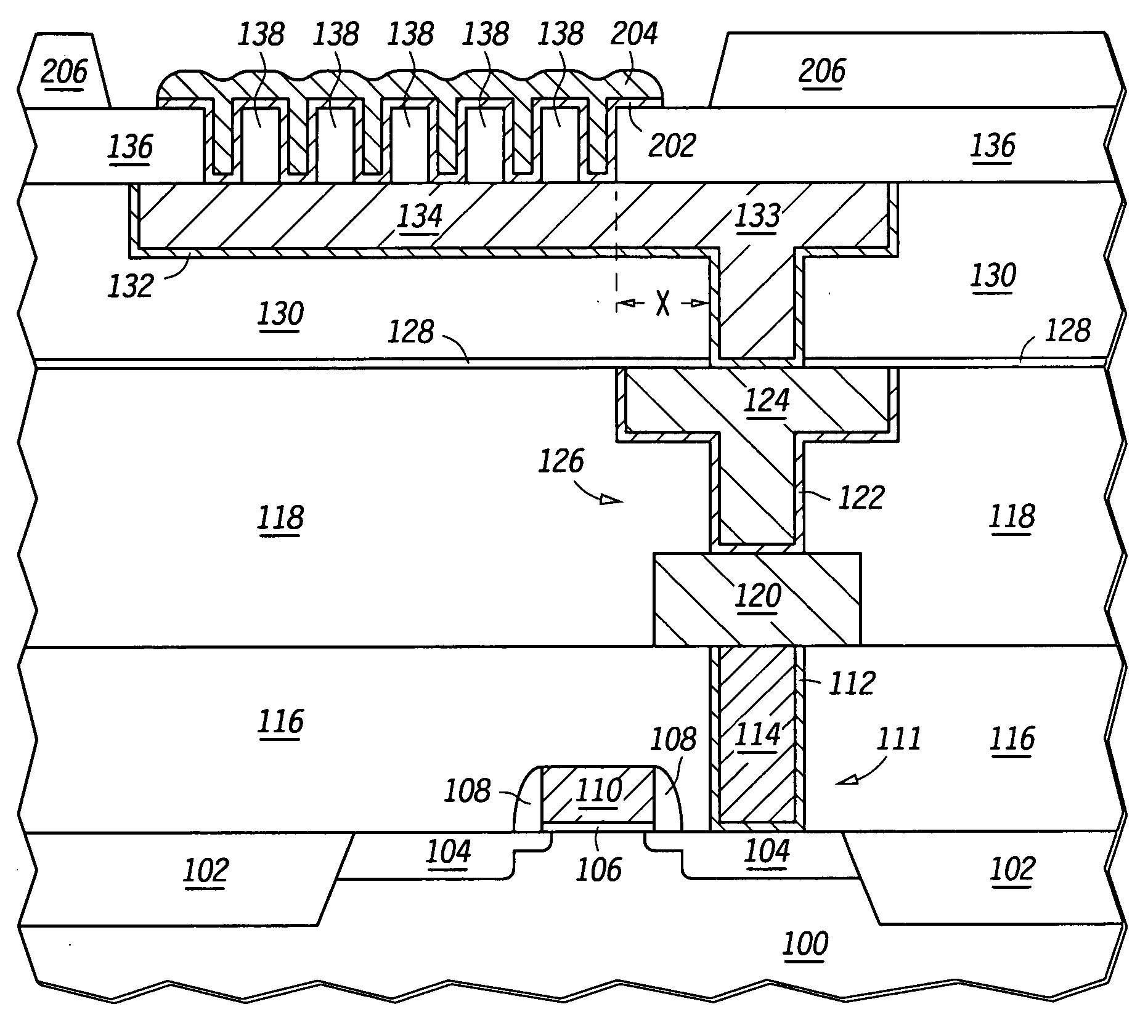
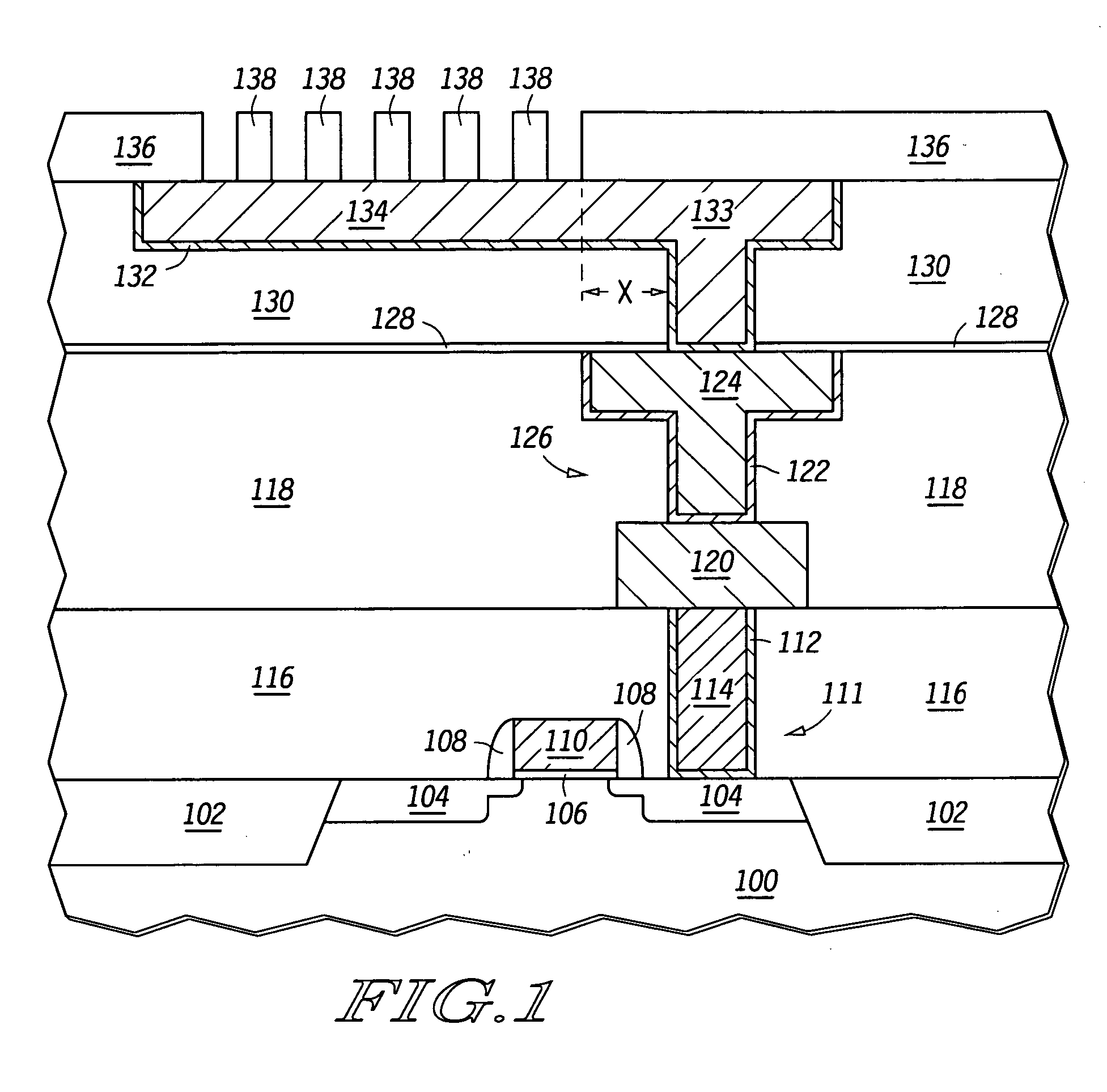
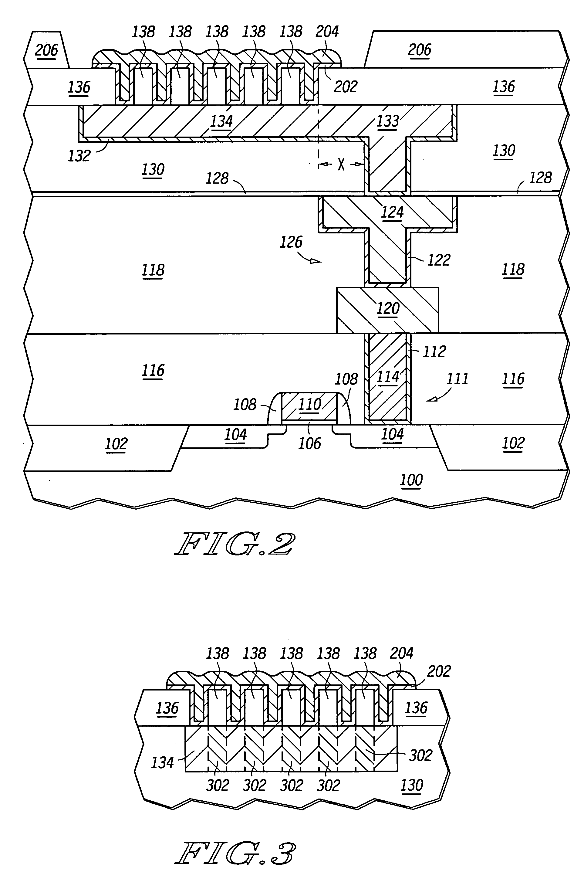
[0017] Generally, the present invention provides a composite bond pad that is resistant to external forces that may be applied during probing operations, packaging operations, or other similar post-fabrication operations that utilize the bond pads. The composite bond pad includes a non-self-passivating conductive bond pad that is formed over a semiconductor substrate. A dielectric layer is then formed over the conductive bond pad. Portions of the dielectric layer are removed such that the dielectric layer becomes perforated and a portion of the conductive bond pad is exposed. Remaining portions of the dielectric ...


PUM


Abstract

A composite bond pad that is resistant to external forces that may be applied during probing or packaging operations is presented. The composite bond pad includes a non-self-passivating conductive bond pad (134) that is formed over a semiconductor substrate (100). A dielectric layer (136) is then formed over the conductive bond pad (134). Portions of the dielectric layer (136) are removed such that the dielectric layer (136) becomes perforated and a portion of the conductive bond pad (134) is exposed. Remaining portions of the dielectric layer (136) form support structures (138) that overlie that bond pad. A self-passivating conductive capping layer (204) is then formed overlying the bond pad structure, where the perforations in the dielectric layer (136) allow for electrical contact between the capping layer (204) and the exposed portions of the underlying bond pad (134). The support structures (138) provide a mechanical barrier that protects the interface between the capping layer (204) and the bond pad (134). Additional mechanical robustness is achieved when the support structures (138) remain coupled to the unremoved portion of the dielectric layer (136), as forces buffered by the support structures (138) are distributed across the dielectric layer (136) and not concentrated at the bond pad location.

Description

RELATED APPLICATIONS [0001] The present Application is related to U.S. patent application Ser. No. 09 / 411,266 filed Oct. 4, 1999, and entitled “Semiconductor Device and Method of Formation,” which is assigned to the assignee hereof and is herein incorporated by reference.FIELD OF THE INVENTION [0002] The invention relates generally to integrated circuits and more particularly to a mechanically robust bond pad interface used in integrated circuits. BACKGROUND OF THE INVENTION [0003] Integrated circuits are formed on semiconductor substrates using a number of different processing operations that create the circuit elements. In order to access circuitry associated with the semiconductor substrate, bond pads are formed on the integrated circuits. Bond pads provide the means for transfer of electrical signals and power from and to the die via probe needles, bonding wires, conductive bumps, etc. [0004] Bond pads are typically formed of a conductive metal such as aluminum, copper, or some ...

Claims


Application Information

Patent Timeline
IPC IPC(8): H01L21/3205H01L21/60H01L21/768H01L23/485H01L23/52
CPCH01L24/03H01L2224/0401H01L24/11H01L2224/05093H01L2224/05166H01L2224/05171H01L2224/05181H01L2224/05184H01L2224/05187H01L2224/05558H01L2224/05624H01L2224/05655H01L2224/05669H01L2224/13099H01L2924/01004H01L2924/01005H01L2924/01006H01L2924/01007H01L2924/01012H01L2924/01013H01L2924/01014H01L2924/01015H01L2924/01016H01L2924/01022H01L2924/01028H01L2924/01029H01L2924/01033H01L2924/01046H01L2924/01073H01L2924/01074H01L2924/01078H01L2924/01082H01L2924/01327H01L2924/014H01L2924/04941H01L2924/04953H01L2924/0496H01L2924/05042H01L2924/14H01L2924/3025H01L24/05H01L2224/05559H01L2924/01024H01L2924/00014H01L21/768
Inventor POZDER, SCOTT K.KOBAYASHI, THOMAS S.
Owner NXP USA INC
Why Eureka
Try Eureka