Method for manufacturing and batch testing semiconductor devices

a technology of semiconductor devices and test apparatuses, applied in semiconductor/solid-state device testing/measurement, instruments, heat measurement, etc., can solve the problems of increasing the production cost of ic sockets, raising the price of devices, and increasing the cost of functional tests. , to achieve the effect of high durability

Inactive Publication Date: 2005-04-12
LAPIS SEMICON CO LTD
View PDF37 Cites 5 Cited by
  • Summary
  • Abstract
  • Description
  • Claims
  • Application Information

AI Technical Summary

Benefits of technology

An object of the present invention, which has been completed by addressing the problems of the prior art discussed above, is to provide a semiconductor device test apparatus that can be employed to test semiconductor devices with electrodes provided at a fine pitch and also achieves a high degree of durability. Another object of the present invention is to provide a semiconductor device test apparatus that is capable of batch testing a great number of semiconductor devices.

Problems solved by technology

If the contact durability of the probes is poor, the cost of the functional test is bound to increase, raising the price of the device itself.
However, the following problems are yet to be addressed in functional tests conducted by utilizing IC sockets and functional tests conducted by utilizing probes.
This will inevitably raise the production cost of the IC socket, and may result in a large increase in the device price.
Such restriction on the number of IC sockets that can be mounted at the circuit board ultimately restricts the number of devices that can be tested in a single functional test.
Thus, functional tests conducted on devices utilizing IC sockets in the prior art are not always efficient.
However, probes are secured to the probe card using a resin or the like in the prior art, which requires a large space for securing them.
Thus, it is difficult to increase the number of probes without increasing the probe card size.
Furthermore, as higher integration of devices becomes more common, the pitch of the device pads with which probes come in contact is becoming narrower.
However, it is difficult to reduce the probe pitch in the structure adopted in the prior art.

Method used


Image

  • Method for manufacturing and batch testing semiconductor devices
  • Method for manufacturing and batch testing semiconductor devices
  • Method for manufacturing and batch testing semiconductor devices

Examples


first embodiment

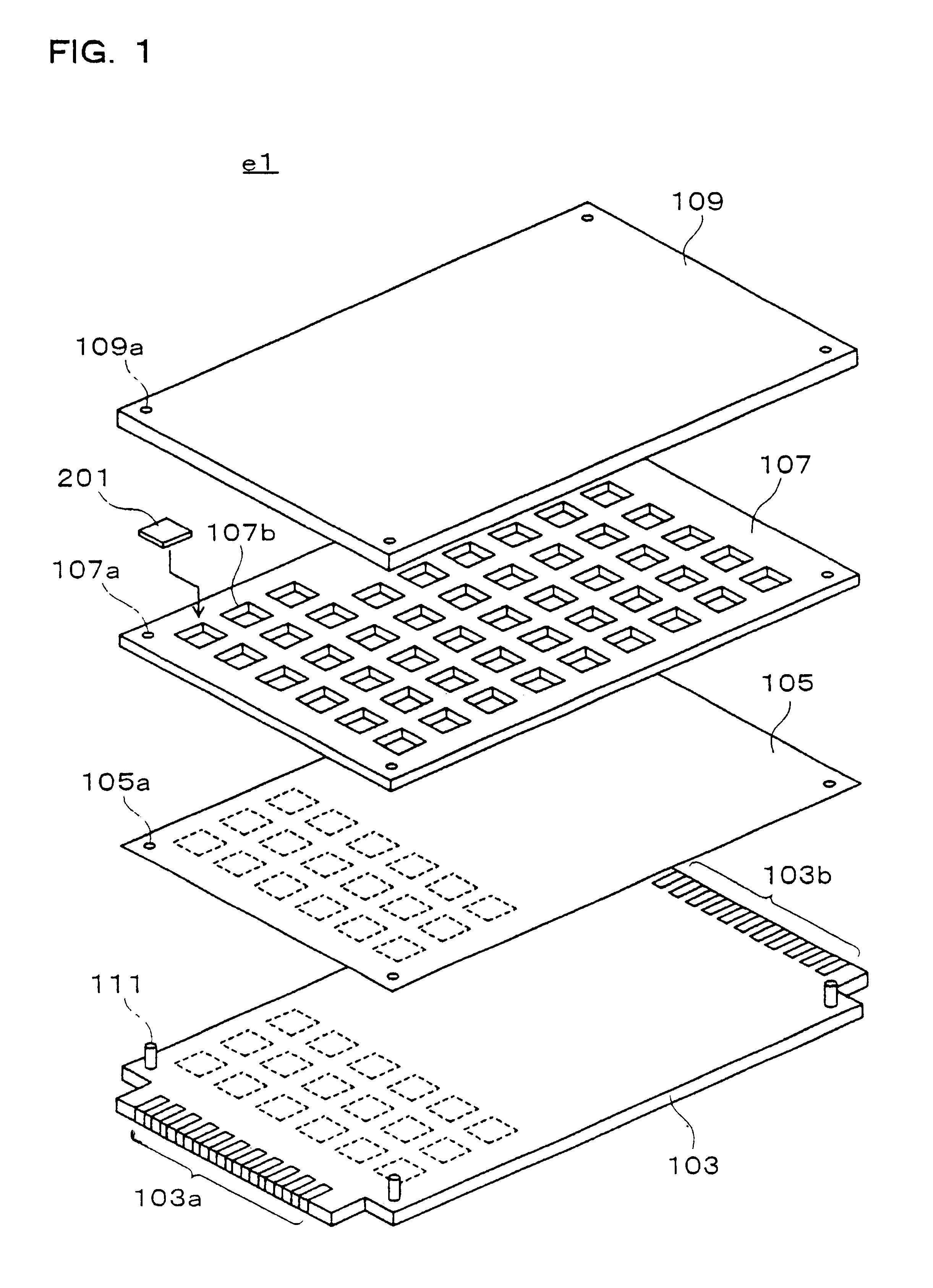
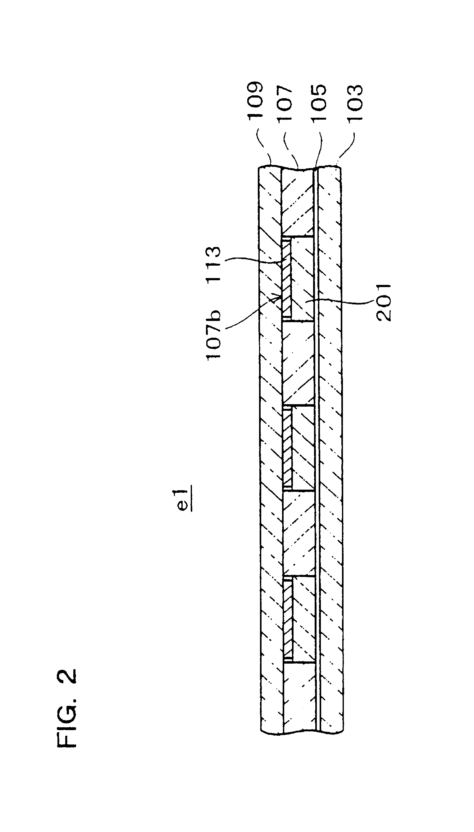
As illustrated in FIG. 1, a semiconductor device test apparatus e1 in the first embodiment of present invention adopts a structure that includes a circuit board 103, a film 105, a positioning plate 107 and a holding plate 109.

The circuit board 103, which is connected to peripheral devices (not shown) via connection terminals 103a and 103b, enables input and output of various types of electrical signals and a source voltage. The circuit board 103 may be constituted of, for instance, a multilayer substrate.

The film 105, the positioning plate 107 and the holding plate 109 are respectively provided with reference holes 105a, 107a and 109a at the four corners, and they are secured onto the circuit board 103 by pins 111.

The positioning plate 107 is provided with a plurality of through holes 107b constituting positioning members so that it can align devices to be measured 201. The through holes 107b are formed in a shape that corresponds to the external shape of the devices to be measured ...

second embodiment

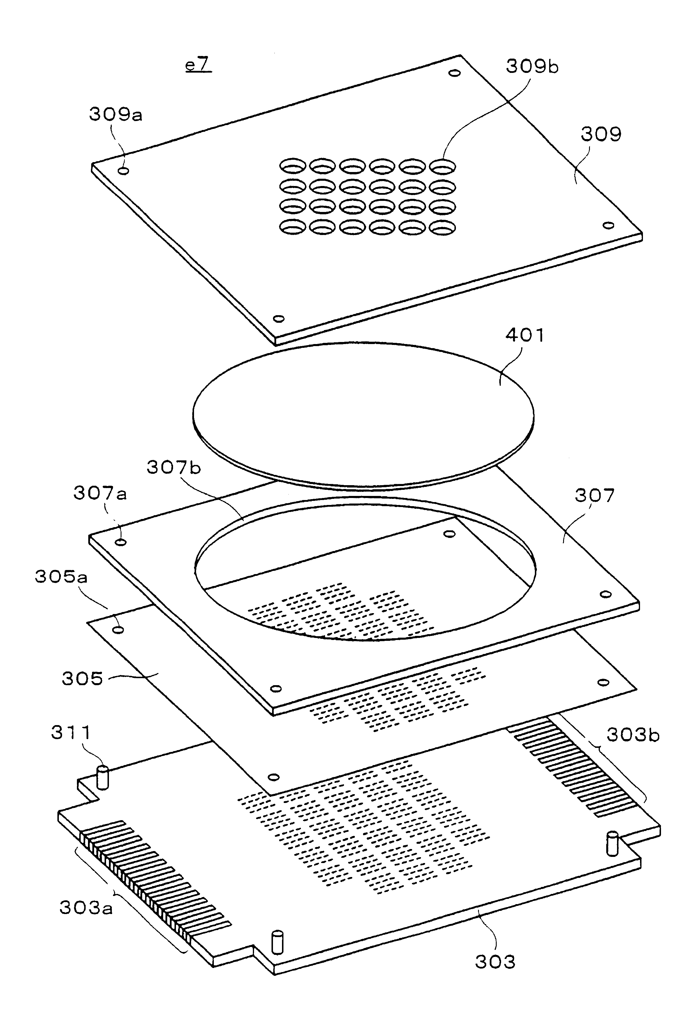
FIG. 4 is a sectional view illustrating a semiconductor device test apparatus e2 in the second embodiment of the present invention and a plurality of devices to be measured 201 that are fitted at the semiconductor device test apparatus e2 for the purpose of various types of functional tests. The semiconductor device test apparatus e2 in the second embodiment adopts a structure which is achieved by replacing the film 105 in the semiconductor device test apparatus e1 in the first embodiment with a printed board 115, as illustrated in FIG. 4.

The devices to be measured 201 are each inserted at a through hole 107b at the positioning plate 107 and are held against the printed board 115 by the holding plate 109. In addition, a buffer member 113 is provided between each device to be measured 201 and the holding plate 109 to ensure that the pressure from the holding plate 109 is distributed to the individual devices to be measured 201 evenly and correctly. Furthermore, the printed board 115 ...

third embodiment

A semiconductor device test apparatus e3 in the third embodiment of the present invention assumes a structure that includes the circuit board 103, the printed board 115, the positioning plate 107, the holding plate 109 and the buffer member 113 that constitute the semiconductor device test apparatus e2 in the second embodiment, as illustrated in FIG. 6.

However, in the semiconductor device test apparatus e3 in the third embodiment, the circuit board 103, the printed board 115 and the positioning plate 107 are integrated to constitute a first unit 121, and the holding plate 109 and the buffer member 113 are integrated to constitute a second unit 122.

When conducting a functional test on the devices to be measured 201, the devices to be measured 201 are each housed inside a device-securing portion 121a which is created by a through hole 107b at the positioning plate 107 constituting the first unit 121. The devices to be measured 201 are pressed down by the second unit 122 to be electric...


PUM

PropertyMeasurementUnit
shapeaaaaaaaaaa
electricalaaaaaaaaaa
conductiveaaaaaaaaaa

Abstract

A semiconductor device test apparatus according to the present invention includes a circuit board 103 and a film 105. A plurality of electrodes 103c are formed at the circuit board 103 at positions that face opposite a plurality of electrodes 201a at a device to be measured 201, whereas bumps 105b are formed at the surface of the film 105 located toward the device to be measured 201, at positions that face opposite the plurality of electrodes 201a at the device to be measured 201 and electrodes 105c are formed at the surface of the film 105 located toward the circuit board 103 at positions that face opposite the plurality of electrodes 103c at the circuit board 103. The bumps 105b formed at one surface of the film 105 and the electrodes 105c formed at another surface of the film 105 are electrically connected with each other via through holes 105d to support semiconductor devices having electrodes provided at a fine pitch and to improve durability.

Description

BACKGROUND OF THE INVENTIONThe present invention relates to a semiconductor device test apparatus.An IC socket which matches the shape of the device to be measured is employed to test a newly developed device in the prior art. An IC socket, which comes into electrical contact with the device to be measured, fulfills a function as a means for electrical signal communication between a peripheral device and the device to be measured.Now, the IC socket, the device to be measured and the connection between the IC socket and the device to be measured are explained in reference to FIGS. 29, 30 and 31.FIG. 29 is a sectional view of a device to be measured 1 and an IC socket 3 mounted at a circuit board 5, illustrating the connections among them. The IC socket 3 is provided with a plurality of contacts 3a, and is soldered onto the circuit board 5 at the contacts 3a. The device to be measured 1, which is pressed down by a holding member 7, is electrically connected with the contacts 3a of the...

Claims


Application Information

Patent Timeline
Patent Type & Authority Patents(United States)
IPC IPC(8): G01K1/00G01K1/16G01R31/26
CPCG01R31/2863G01K1/16
Inventor OHTAKI, MIKIO
Owner LAPIS SEMICON CO LTD
Why Eureka
Try Eureka