Film forming method and film forming apparatus
a film forming and film technology, applied in electrical devices, semiconductor devices, semiconductor/solid-state device details, etc., can solve the problems of poor adhesion of dielectric constant insulation film and insulation film as etching mask and chemical mechanical polishing stopper, poor adhesion of inorganic type film and organic type film, etc., to achieve the effect of improving adhesion
- Summary
- Abstract
- Description
- Claims
- Application Information
AI Technical Summary
Benefits of technology
Problems solved by technology
Method used
Image

Examples
second embodiment
[0086] In addition, as a flow chart showing a processing flow in the second embodiment, the surface reforming process in the surface reforming process station 70 is applied in step 2 and step 8 shown in FIG. 7.
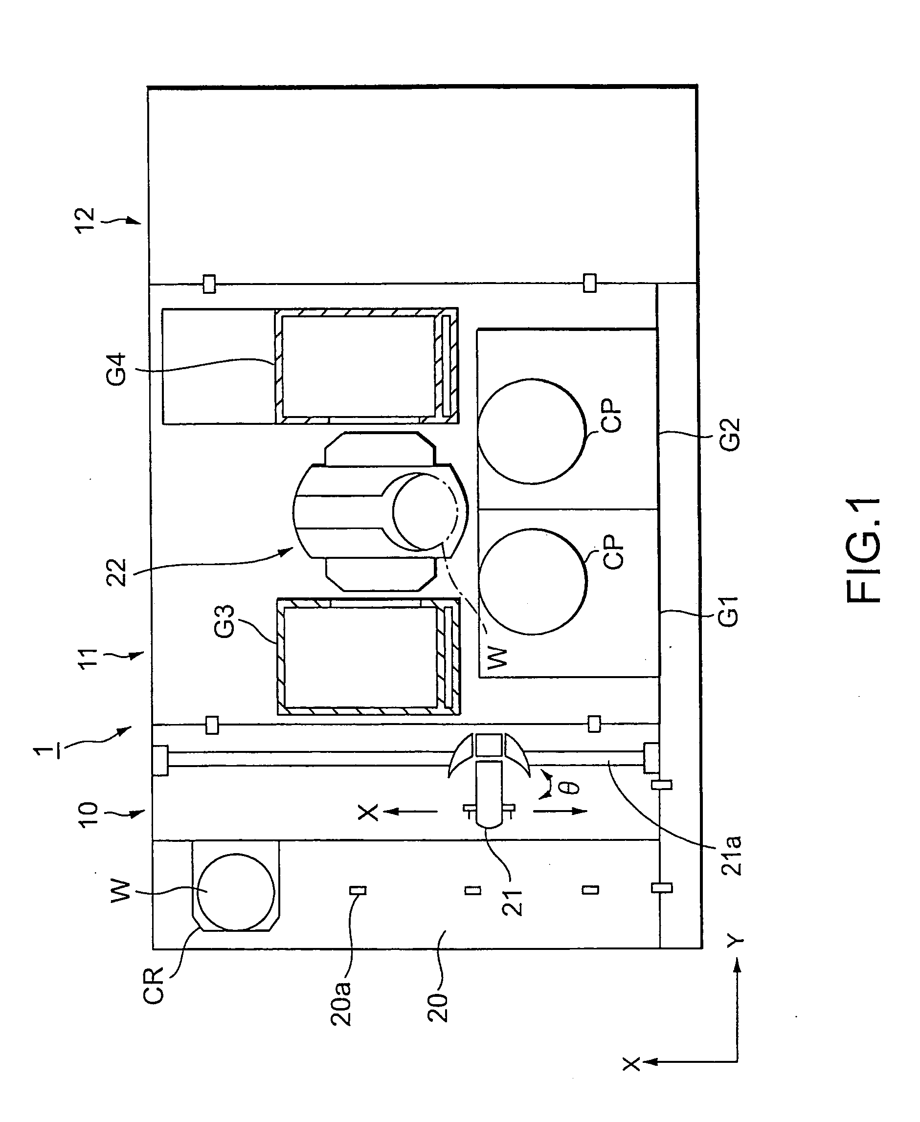
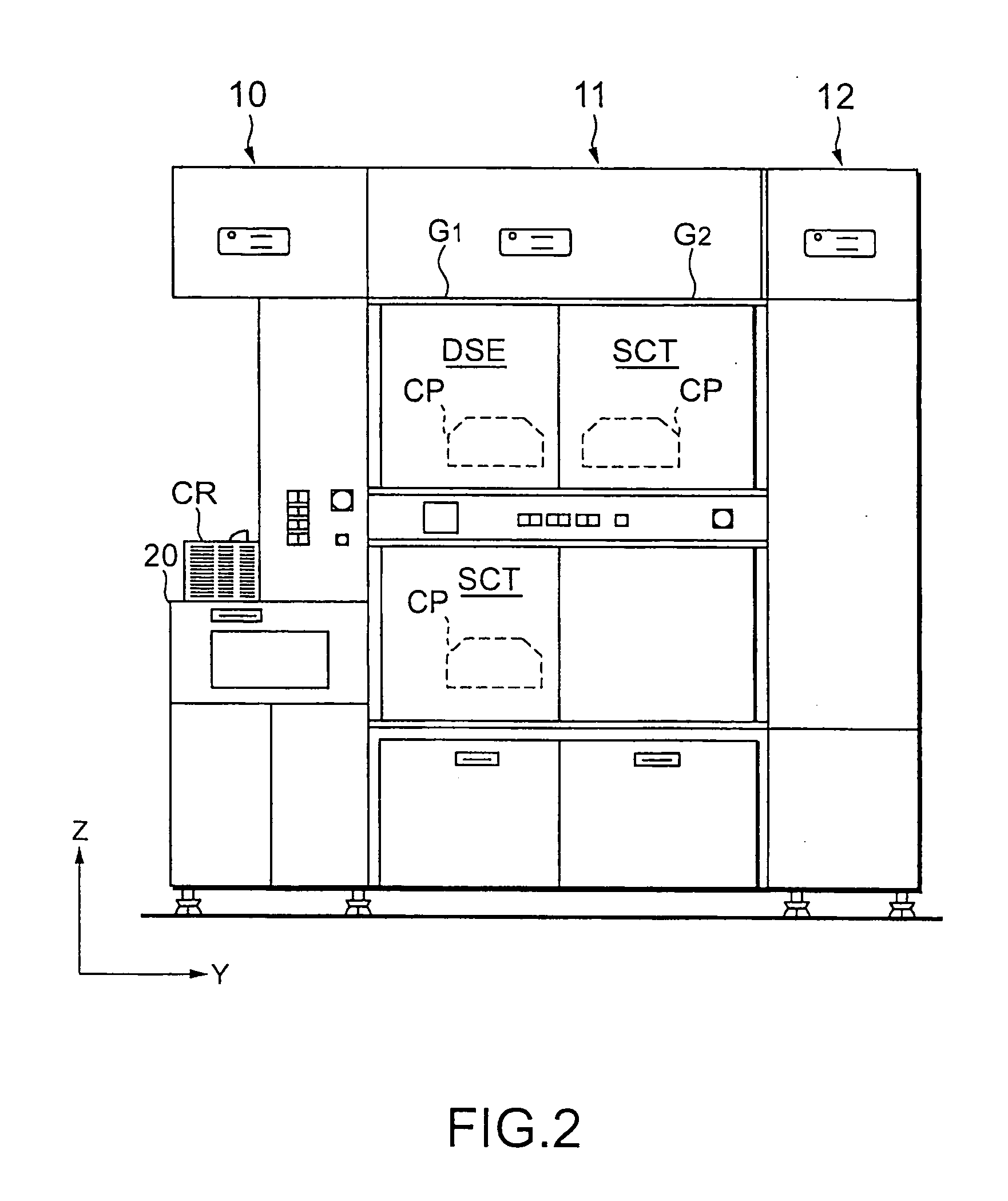
[0087]FIG. 13 and FIG. 14 are a plan view and a sectional view respectively of the surface reforming process station 50 according to another embodiment. Same symbols as in FIG. 4, FIG. 5 and FIG. 12 are used for the same structure corresponding to FIG. 13 and FIG. 14 and an explanation thereof is omitted.
[0088] In the surface reforming process station 90 of the present embodiment, a high-density plasma generating apparatus 92 is provided to be able to move along a guide rail 93 in Y-direction. The high-density plasma generating apparatus 92 is a high-density plasma generating apparatus using, for example, ICP (Inductively Coupled Plasma). And a shutter 94 is provided at an opening 98 that is used for transferring the wafer W to and from the arm 31, capable of hermetically sea...
first embodiment
[0108] The reforming process by the surface reforming process station 50 of parallel plate type in the first embodiment mentioned above is performed under reduced pressure state, however, the process can also be performed under normal pressure.
[0109] Furthermore, each of the embodiments described above is not limited to the application to a semi-conductor wafer processing system, however, the present invention can also be applied to a system processing a glass substrate used with liquid crystal display and the like.
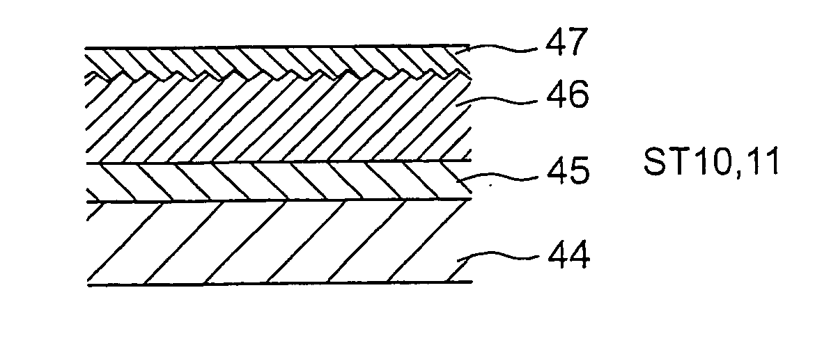
[0110] As described above, according to the present invention, regardless of an organic type and inorganic type insulation film, an inorganic film on which the hydrophobic process is being performed, a SiOF film etc. adhesion between the films and also between the inter-layer insulation film and other neighboring film can be improved.
PUM
| Property | Measurement | Unit |
|---|---|---|
| dielectric constant | aaaaa | aaaaa |
| dielectric constant | aaaaa | aaaaa |
| pressure | aaaaa | aaaaa |
Abstract
Description
Claims
Application Information
 - R&D Engineer
- R&D Manager
- IP Professional
- Industry Leading Data Capabilities
- Powerful AI technology
- Patent DNA Extraction
Browse by: Latest US Patents, China's latest patents, Technical Efficacy Thesaurus, Application Domain, Technology Topic.
© 2024 PatSnap. All rights reserved.Legal|Privacy policy|Modern Slavery Act Transparency Statement|Sitemap