

Automatic transmission line pulse system
a transmission line and pulse system technology, applied in the direction of transmission systems, individual semiconductor device testing, instruments, etc., can solve the problems of inability to take conjunctively esd characteristics at the gate or substrate, damage or destruction of ic, and hbm and mm build-up
- Summary
- Abstract
- Description
- Claims
- Application Information
AI Technical Summary
Benefits of technology
Problems solved by technology
Method used
Image

Examples
Embodiment Construction
[0002] 1. Field of the Invention
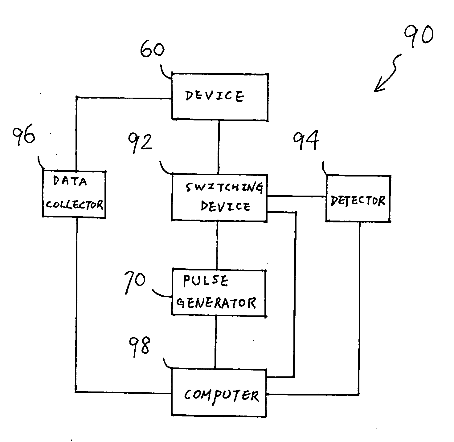
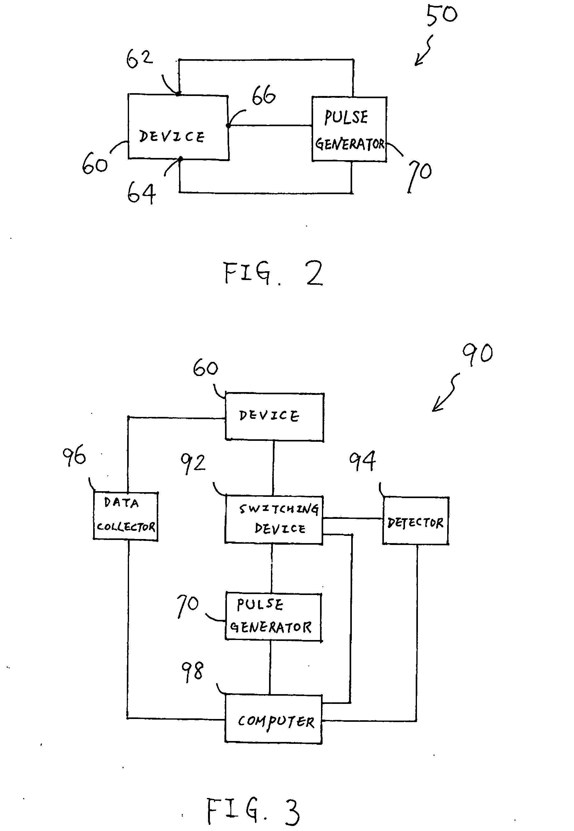
[0003] This invention pertains in general to measurement of electrical characteristics of a semiconductor device and, more particularly, to systems and methods for measuring ESD characteristics in a semiconductor device.
[0004] 2. Background of the Invention
[0005] A semiconductor integrated circuit (“IC”) is generally susceptible to an electrostatic discharge (“ESD”) event, which may damage or destroy the IC. An ESD event is an electrical discharge of a current (positive or negative) for a short duration during which a large amount of current is provided to the IC. The high current may be built-up from a variety of sources, such as the human body and machines, referred to as the human body model (“HBM”) and machine model (“MM”), respectively. An IC is particularly susceptible to the HBM and MM built-up during fabrication, transportation, or handling.
[0006] Conventional ESD protection devices manufactured with complementary metal-oxide-semiconductor...
PUM
| Property | Measurement | Unit |
|---|---|---|
| leakage current | aaaaa | aaaaa |
| electrical characteristics | aaaaa | aaaaa |
| current | aaaaa | aaaaa |
Abstract
Description
Claims
Application Information