Semiconductor device and method for manufacturing semiconductor device

a semiconductor and semiconductor technology, applied in the field of semiconductor devices, can solve problems such as increasing base resistan

Inactive Publication Date: 2005-02-17
KK TOSHIBA
View PDF8 Cites 16 Cited by
  • Summary
  • Abstract
  • Description
  • Claims
  • Application Information

AI Technical Summary

Benefits of technology

[0008] A feature of the present invention inheres in a semiconductor device including: a collector region having a first conductivity type; an intrinsic base region having a second conductivity type provided on the collector region; an emitter region having the first conductivity type formed in an upper section of the intrinsic base region; an isolation region provided on a side of the collector region directly under the intrinsic base region; an extrinsic base region having the second conductivity type provided adjacent to the intrinsic base region, and having a higher impurity concentration than the intrinsic base region; and a base electrode region provided on the isolation region, and contacting a side of the extrinsic base region so as to have a region at the same level as the intrinsic base region.

Problems solved by technology

However, when the collector junction area is reduced, the junction area between the extrinsic base region and the base electrode region is reduced as well, thus there is problem of increasing base resistance.

Method used


Image

  • Semiconductor device and method for manufacturing semiconductor device
  • Semiconductor device and method for manufacturing semiconductor device
  • Semiconductor device and method for manufacturing semiconductor device

Examples


Embodiment Construction

[0015] Various embodiments of the present invention will be described with reference to the accompanying drawings. It is to be noted that the same or similar reference numerals are applied to the same or similar parts and elements throughout the drawings, and the description of the same or similar parts and elements will be omitted or simplified.

[0016] Generally and as it is conventional in the representation of semiconductor devices, it will be appreciated that the various drawings are not drawn to scale from one figure to another nor inside a given figure, and in particular that the layer thicknesses are arbitrarily drawn for facilitating the reading of the drawings.

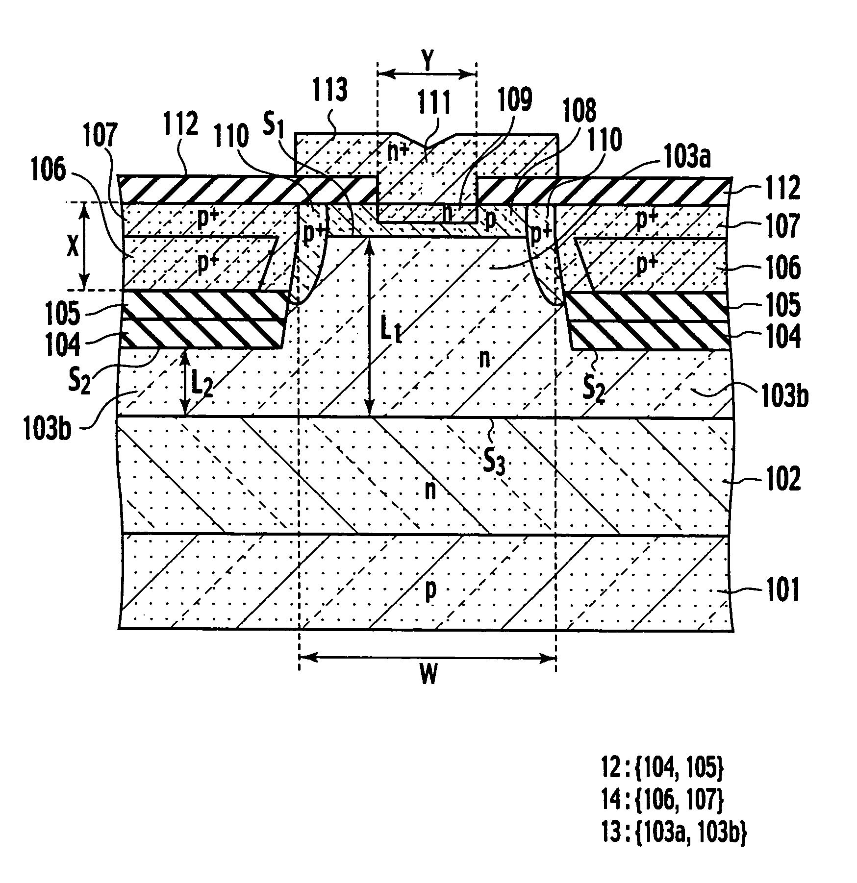
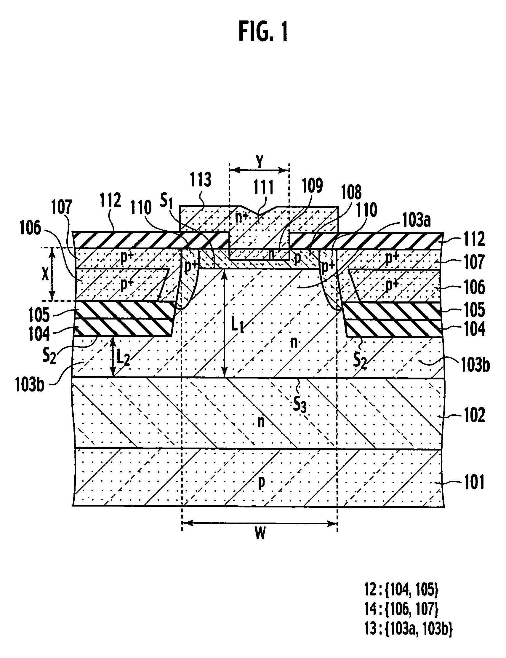
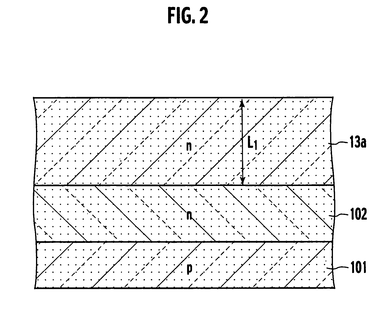
[0017] In the embodiment of the present invention, the “first conductivity type” and “second conductivity type” are mutual opposites. In other words, when the first conductivity type is an n-type then the second conductivity type will be a p-type, and vice versa. Below, a pnp bipolar junction transistor with the firs...


PUM


Abstract

A semiconductor device includes: a collector region having a first conductivity type; an intrinsic base region having a second conductivity type provided on the collector region; an emitter region having the first conductivity type formed in an upper section of the intrinsic base region; an isolation region provided on a side of the collector region directly under the intrinsic base region; an extrinsic base region having the second conductivity type provided adjacent to the intrinsic base region, and having a higher impurity concentration than the intrinsic base region; and a base electrode region provided on the isolation region, and contacting a side of the extrinsic base region so as to have a region at the same level as the intrinsic base region.

Description

CROSS REFERENCE TO RELATED APPLICATIONS [0001] This application is based upon and claims the benefit of priority from the prior Japanese Patent Applications No. P2003-195310, filed on Jul. 10, 2003; the entire contents of which are incorporated herein by reference. BACKGROUND OF THE INVENTION [0002] 1. Field of the Invention [0003] The present invention relates to a semiconductor device including a bipolar junction transistor and a method for manufacturing the same. [0004] 2. Description of the Related Art [0005] The bipolar junction transistor is known as a semiconductor device for use in high frequency applications. The bipolar junction transistor includes a collector region, an intrinsic base region provided on the collector region, and an emitter region formed in the upper section of the intrinsic base region. An extrinsic base region is provided so as to surround the intrinsic base region. A base electrode region is provided on the top of the extrinsic base region. [0006] In or...

Claims


Application Information

Patent Timeline
Patent Type & Authority Applications(United States)
IPC IPC(8): H01L21/331H01L29/06H01L29/08H01L29/10H01L29/417H01L29/732H01L29/737
CPCH01L29/0649H01L29/0804H01L29/0821H01L29/732H01L29/41708H01L29/66287H01L29/1004
Inventor MASUDA, KEITA
Owner KK TOSHIBA
Why Eureka
Try Eureka